A method for preparing surface-enhanced Raman substrates by improving the binding force of membrane substrates

A surface-enhanced Raman and film-substrate bonding technology, which is applied in the direction of superimposed layer plating, vacuum evaporation plating, coating, etc., can solve the problem of weak bonding between noble metal thin films and substrate materials, which affects the practical application of SERS substrates, Limit the development of surface-enhanced Raman technology and other issues, and achieve the effects of improving substrate adhesion, promoting diffusion and interaction, and excellent stability

Active Publication Date: 2020-05-12
广西三环高科拉曼芯片技术有限公司
View PDF2 Cites 0 Cited by
  • Summary
  • Abstract
  • Description
  • Claims
  • Application Information

AI Technical Summary

Problems solved by technology

When nanoparticles are deposited on the surface of silicon substrates, glass substrates, organic substrates, etc., the bonding force between the noble metal film and the substrate material is often weak, so that the nanofilm falls off from the substrate during transportation, use and storage. It affects the practical application of SERS substrates and greatly limits the development of surface-enhanced Raman technology

Method used


Image

  • A method for preparing surface-enhanced Raman substrates by improving the binding force of membrane substrates
  • A method for preparing surface-enhanced Raman substrates by improving the binding force of membrane substrates
  • A method for preparing surface-enhanced Raman substrates by improving the binding force of membrane substrates

Examples


Embodiment 1

[0026] 1).Use acetone, alcohol, and deionized water to ultrasonically clean silicon substrates, glass, and other substrates in sequence and dry them in the air;

[0027] 2). Fix the cleaned substrate on the sample stage of the electron beam evaporation coating machine, and pump the chamber of the coating machine to a vacuum degree of 10 -5 Pa level;

[0028] 3). Using metal Ti as the target material, a transition layer film is plated on the substrate, and the incident angle of the electron beam is adjusted to 0°, and the evaporation rate of Ti is The deposition thickness is 15nm;

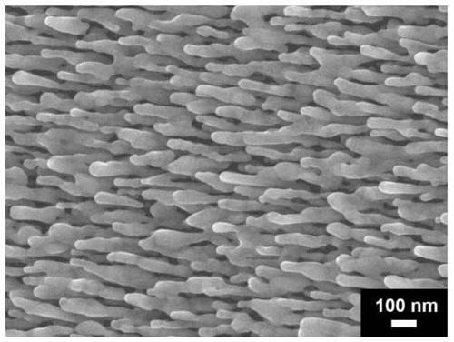
[0029] 4). Using metallic Ag as the target material, plate an Ag nanorod array thin film on the transition layer, adjust the incident angle of the electron beam to 85°, and make the sample stage static, and grow inclined silver nanorods with a nanorod length of 700nm array film;

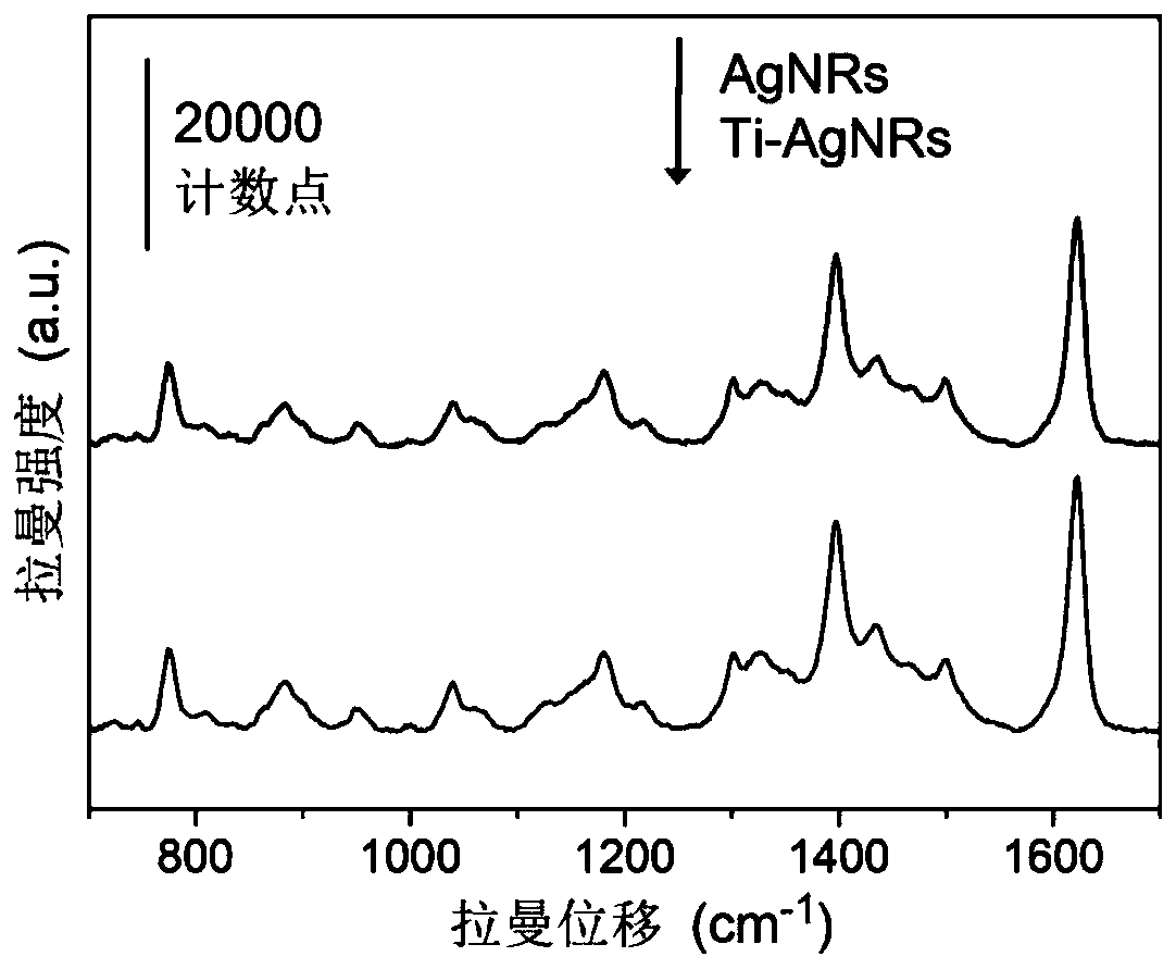
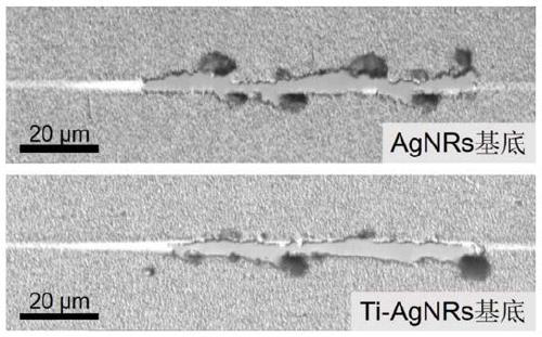
[0030] 5).Using the nano-scratch method to evaluate the film-base bonding force of the film, a diamond indenter is u...

Embodiment 2

[0035] 1).Use acetone, alcohol, and deionized water to ultrasonically clean silicon substrates, glass, and other substrates in sequence and dry them in the air;

[0036] 2). Fix the cleaned substrate on the sample stage of the electron beam evaporation coating machine, and pump the chamber of the coating machine to a vacuum degree of 10 -5 Pa level;

[0037] 3). Using metal Ti as the target material, a transition layer film is plated on the substrate, and the incident angle of the electron beam is adjusted to 0°, and the evaporation rate of Ti is The deposition thickness is 25nm;

[0038] 4). Using metallic Ag as the target material, plate an Ag nanorod array thin film on the transition layer, adjust the incident angle of the electron beam to 86°, and make the sample stage static, and grow obliquely inclined silver nanorods with a nanorod length of 800nm array film;

[0039] 5).Using low-temperature atomic layer deposition technology, set the reaction chamber temperature o...

Embodiment 3

[0045] 1).Use acetone, alcohol, and deionized water to ultrasonically clean silicon substrates, glass, and other substrates in sequence and dry them in the air;

[0046] 2). Fix the cleaned substrate on the sample stage of the electron beam evaporation coating machine, and pump the chamber of the coating machine to a vacuum degree of 10 -5 Pa level;

[0047] 3). Using metal TiN as the target material, a transition layer film is plated on the substrate, and the incident angle of the electron beam is adjusted to 0°, and the evaporation rate of TiN is The deposition thickness is 40nm;

[0048] 4). Using metallic Ag as the target material, plate an Ag nanorod array thin film on the transition layer, adjust the incident angle of the electron beam to 87°, and make the sample stage static, and grow obliquely inclined silver nanorods with a nanorod length of 900nm array film;

[0049] 5).Using low-temperature atomic layer deposition technology, set the temperature of the reaction ...


PUM

PropertyMeasurementUnit
thicknessaaaaaaaaaa
thicknessaaaaaaaaaa
thicknessaaaaaaaaaa

Abstract

The invention relates to a method for preparing a surface-enhanced Raman substrate by improving film-substrate bonding force. The method comprises the following steps of firstly, growing a flat transition layer on a substrate; growing a silver nanorod array thin film on the transition layer; uniformly covering the surface of silver with an ultrathin oxide film; heating the composite nanometer structure, so as to obtain the surface-enhanced Raman substrate with excellent film-substrate bonding force. The method has the advantages that the mismatching factor between the noble metal thin film andthe substrate is relieved by the transition layer, and the stress distribution and atom bonding in the whole film-substrate range are regulated; the good SERS (surface enhanced Raman scattering) sensitivity and thermal stability of the substrate are ensured by the ultrathin oxide layer at the surface of the silver nanorod; the substrate can be further heated, the atom diffusion between the thin film and the substrate can be promoted, the porosity at the interface is reduced, and the adhesion force is increased. The surface-enhanced Raman substrate with excellent film-substrate bonding force has the advantages that the easiness in falling is avoided, the stability is good, the transportation, storage and use are convenient, and the practicality of surface-enhanced Raman technique is enhanced.

Description

technical field [0001] The invention belongs to the technical field of trace substance detection, and in particular relates to a method for preparing a surface-enhanced Raman substrate by improving the binding force of a membrane substrate. Background technique [0002] Surface-enhanced Raman scattering (SERS) can amplify the Raman scattering signal of adsorbed molecules by several orders of magnitude, so it can be used for highly sensitive detection of trace substances, with fingerprint recognition, fast detection, and easy Line, good selectivity and non-destructive testing and other advantages. [0003] The surface-enhanced Raman effect requires the use of gold, silver and other noble metal nanostructures as highly sensitive enhanced substrates. The preparation methods include electrochemical redox method, metal sol method, template method, self-assembly method, electron beam lithography method, tilt angle deposition method, etc. When nanoparticles are deposited on the s...

Claims


Application Information

Patent Timeline
Patent Type & Authority Patents(China)
IPC IPC(8): C23C14/06C23C14/16C23C14/18C23C14/30C23C16/40C23C28/00C23C16/56
CPCC23C14/0641C23C14/16C23C14/18C23C14/30C23C16/403C23C16/405C23C16/56C23C28/322C23C28/3455
Inventor 张政军马菱薇
Owner 广西三环高科拉曼芯片技术有限公司
Why Eureka
Try Eureka