
A kind of array substrate, touch display panel and touch display panel driving method

A technology for array substrates and display areas, applied in character and pattern recognition, instruments, fingerprint/palmprint acquisition/organization, etc., can solve the problems of increased non-display area occupation area, complicated electronic equipment circuits, etc., to avoid new The effect of fingerprint control circuit and circuit simplification

Active Publication Date: 2020-05-01
WUHAN TIANMA MICRO ELECTRONICS CO LTD
View PDF4 Cites 0 Cited by
  • Summary
  • Abstract
  • Description
  • Claims
  • Application Information

AI Technical Summary

Problems solved by technology

[0005] In view of this, the present invention provides an array substrate, a touch display panel, and a touch display panel driving method to solve the need to add a fingerprint identification control circuit in the prior art for fingerprint identification, which causes the circuit of the electronic device to be complicated and non-display The problem of increased area footprint

Method used


Image

  • A kind of array substrate, touch display panel and touch display panel driving method
  • A kind of array substrate, touch display panel and touch display panel driving method
  • A kind of array substrate, touch display panel and touch display panel driving method

Examples


Embodiment Construction

[0044] The following will clearly and completely describe the technical solutions in the embodiments of the present invention with reference to the accompanying drawings in the embodiments of the present invention. Obviously, the described embodiments are only some, not all, embodiments of the present invention. Based on the embodiments of the present invention, all other embodiments obtained by persons of ordinary skill in the art without making creative efforts belong to the protection scope of the present invention.

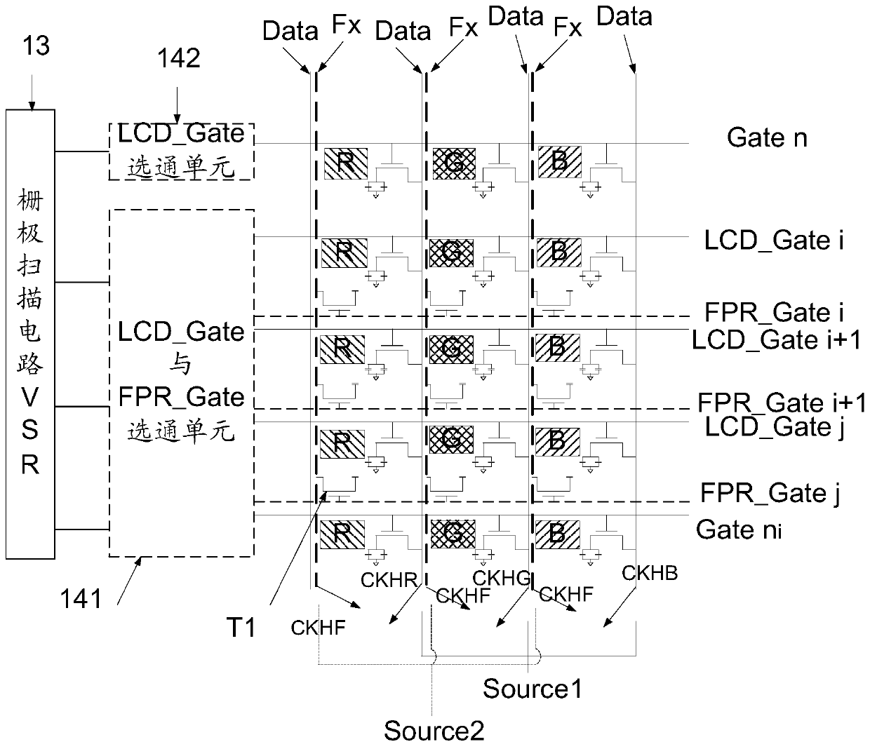
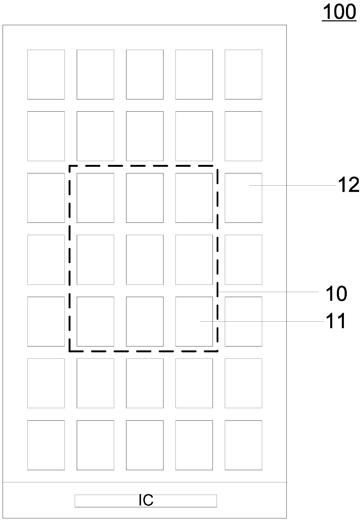
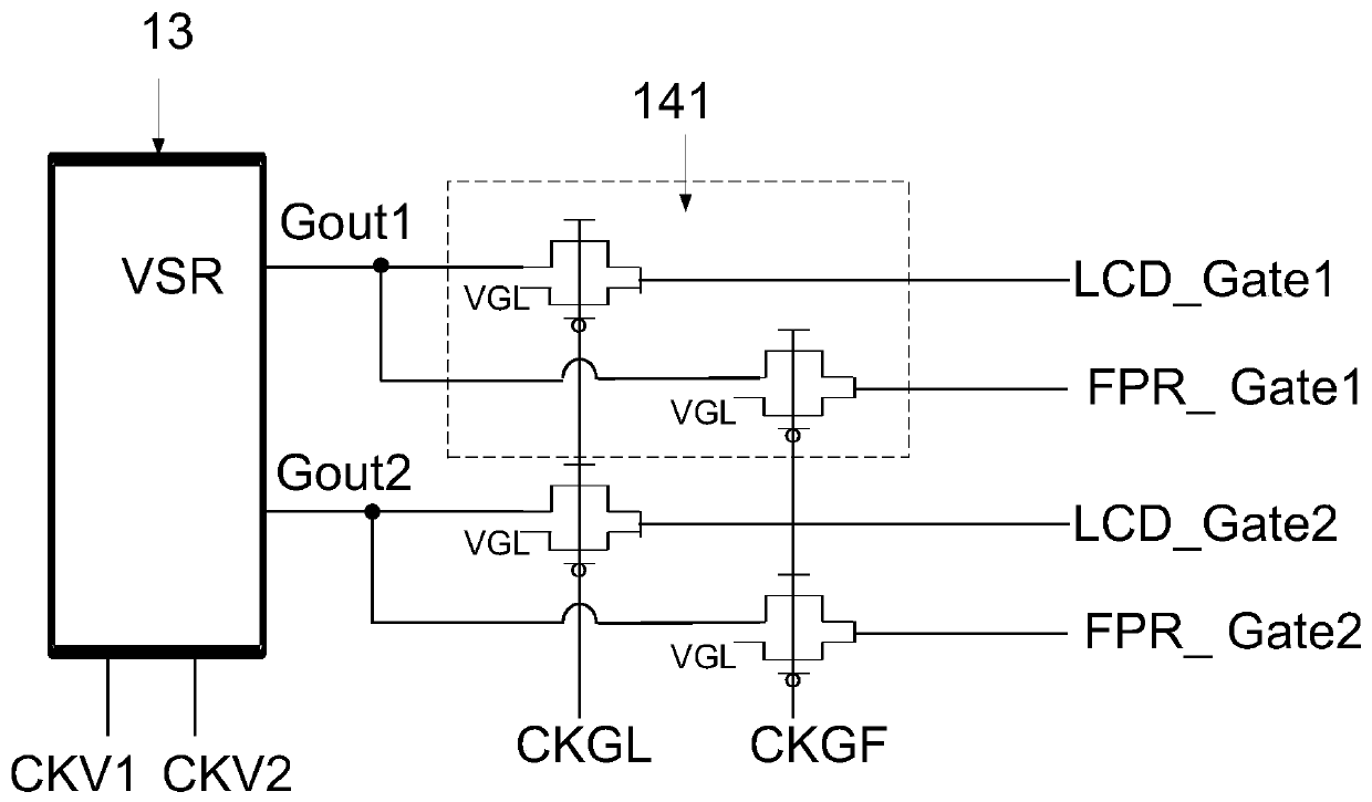
[0045] See figure 1 and figure 2 , the present invention provides an array substrate 100, including: a substrate, the substrate includes a display area; a plurality of scanning lines LCD_Gate and a plurality of data lines Data located on the substrate, and a plurality of scanning lines LCD_Gate and a plurality of data lines Data intersect And the insulating arrangement defines a plurality of sub-pixels arranged in a matrix. A plurality of touch electrodes a...


PUM


Abstract

The present application provides an array substrate, a touch display panel, and a touch display panel driving method. The array substrate includes a plurality of fingerprint detection areas in the predetermined area of ​​the display area of ​​the substrate, and the substrate also includes a plurality of fingerprints. Scanning lines, the fingerprint sensing unit in the fingerprint detection area is connected to the fingerprint scanning line through the first switch tube, and each fingerprint scanning line and each scanning line are connected to the grid scanning circuit through the gate unit, so that the fingerprint detection area is in the The first time period is used for display, and the second time period is used for fingerprint detection. That is to say, in the present invention, a new fingerprint scanning line is added, and through the gating unit and the gate scanning circuit, the control of the fingerprint sensing unit in the fingerprint detection area can reuse the gate scanning circuit, thereby avoiding adding a new fingerprint control circuit, The circuit of the array substrate is simplified, and the area of ​​the non-display area does not need to be occupied.

Description

technical field [0001] The present invention relates to the field of display technology, in particular to an array substrate, a touch display panel and a driving method for the touch display panel. Background technique [0002] With the development of multimedia technology, portable electronic devices such as smart phones and tablet computers have become necessary tools in people's lives, in which important personal information of users is often stored. Therefore, it is necessary to set up certain identity authentication and rights management measures in the use of such products to protect the information stored in them, so as to prevent users' personal information from being accidentally leaked or stolen. [0003] Among the existing identity authentication methods, fingerprint identification (Fingerprint Identification) is a relatively advanced and widely used method. Since each person's fingerprint is unique, the fingerprint recognition authentication method is highly sec...

Claims


Application Information

Patent Timeline
Patent Type & Authority Patents(China)
IPC IPC(8): G02F1/1333G02F1/1343G06F3/041G06K9/00
CPCG02F1/13338G02F1/1343G06F3/0412G06F3/0416G06V40/1306
Inventor 郭珂王伟鹏杨康鹏许育民吴常志孙莹
Owner WUHAN TIANMA MICRO ELECTRONICS CO LTD
Learn More