
Manufacturing method and structure of asymmetric high-voltage MOS device

A technology of MOS devices and manufacturing methods, which is applied in semiconductor/solid-state device manufacturing, semiconductor devices, electrical components, etc., can solve the problems of narrowing the cross-section of the current path, increasing the equivalent path resistance, and reducing the driving current. Effects of equivalent path resistance, increased drive current, and convenient lateral size

Active Publication Date: 2014-10-08
SHANGHAI HUAHONG GRACE SEMICON MFG CORP
View PDF4 Cites 0 Cited by
  • Summary
  • Abstract
  • Description
  • Claims
  • Application Information

AI Technical Summary

Problems solved by technology

However, a problem caused by the high doping concentration of the P well in the body region is that, since the P well is connected to the source region on the side of the source region, the lateral diffusion of the P well will make the source end That is, the cross-section of the current path on the source region side becomes narrower, that is, the equivalent path resistance at the source end becomes larger, so that the driving current of the device is relatively small

Method used


Image

  • Manufacturing method and structure of asymmetric high-voltage MOS device
  • Manufacturing method and structure of asymmetric high-voltage MOS device
  • Manufacturing method and structure of asymmetric high-voltage MOS device

Examples


Embodiment Construction

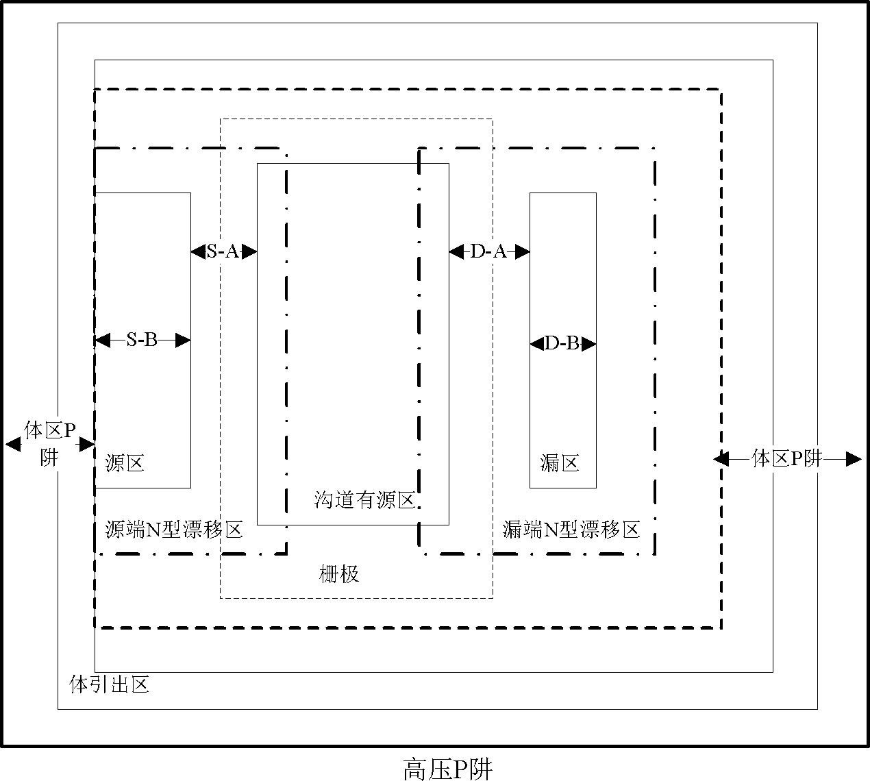
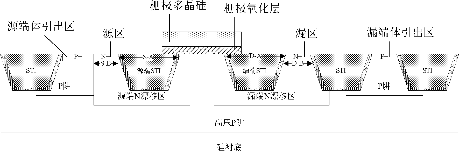
[0023] The present invention will be further described below with reference to the manufacturing method and structure of the asymmetric high-voltage NMOS device of the embodiment of the present invention. For the manufacturing method and structure of the asymmetric high-voltage PMOS device, the doping types of the body region, drift region, and source-drain region are just opposite to those of the asymmetric high-voltage NMOS device, so this patent does not make further descriptions.

[0024] Such as figure 2 Shown is a schematic diagram of the structure of an asymmetric high-voltage NMOS device according to an embodiment of the present invention. The method for manufacturing an asymmetric high-voltage NMOS device according to an embodiment of the present invention includes the following steps:

[0025] Step 1: Change the layout during the layout design process. Such as figure 1 Shown, the embodiment method of the present invention and figure 1 The only difference in the ...


PUM


Abstract

The invention discloses a manufacturing method of an asymmetrical high-voltage MOS (metal oxide semiconductor) device. The method comprises the following steps of: adjusting the sizes of the shallow trench isolation areas of the source region and the source end in a layout design process; keeping the total transverse sizes of the shallow trench isolation areas of the source region and the source end unchanged; reducing the transverse size of the shallow trench isolation area of the source end; increasing the transverse size of the source region; and in a manufacturing process, forming a shallow trench at the source end of the device by use of the layout of the shallow trench isolation area of the source end after the size adjustment. The invention also discloses a structure of an asymmetrical high-voltage MOS device. Through the invention, the equivalent via resistance at the source end is reduced and the drive current of the device is increased under the condition of keeping the total size of the device unchanged.

Description

technical field [0001] The invention relates to the field of manufacturing semiconductor integrated circuits, in particular to a method for manufacturing an asymmetric high-voltage MOS device, and the invention also relates to the structure of an asymmetric high-voltage MOS device manufactured by the method. Background technique [0002] In the structure of the existing asymmetric high-voltage MOS device, the source region and the body region of the corresponding source end are often adjacent to and connected together in order to save area. Existing asymmetric high-voltage NMOS devices are formed in a high-voltage P well on a silicon substrate, and an N-type drift region at the active end, an N-type drift region at the drain end, a P well at the source end, and a P well at the drain end are formed in the high-voltage P well. well; the P well at the source end, the P well at the drain end and the high voltage P well form a body region; the P well at the source end is in conta...

Claims


Application Information

Patent Timeline
Patent Type & Authority Patents(China)
IPC IPC(8): H01L21/336H01L29/78H01L29/06H01L29/08
Inventor 熊涛罗啸陈瑜陈华伦
Owner SHANGHAI HUAHONG GRACE SEMICON MFG CORP
Learn More