

Polishing-caused quartz crystal wafer surface shallow scratch visual detection method
A technology for visual inspection of quartz wafers, applied in image data processing, instruments, calculations, etc., can solve the problem that shallow scratches on the surface of quartz wafers cannot be completely detected, and achieve the effect of inspection quality assurance
- Summary
- Abstract
- Description
- Claims
- Application Information
AI Technical Summary
Problems solved by technology
Method used
Image

Examples
Embodiment Construction
[0029] Before describing the embodiments in detail, it should be understood that the present invention is not limited to the detailed structures or arrangements of elements described herein below or in the accompanying drawings. The present invention can be implemented in other ways. Also, it should be understood that the phraseology and terminology used herein are for descriptive purposes only and should not be interpreted as limiting. The terms "including", "comprising", "having" and similar expressions used herein are meant to include the items listed thereafter, their equivalents and other additional items. In particular, when "a certain element" is described, the present invention does not limit the number of the element to one, but may also include a plurality.
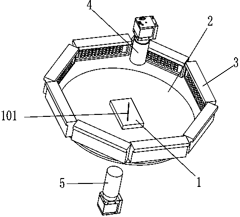
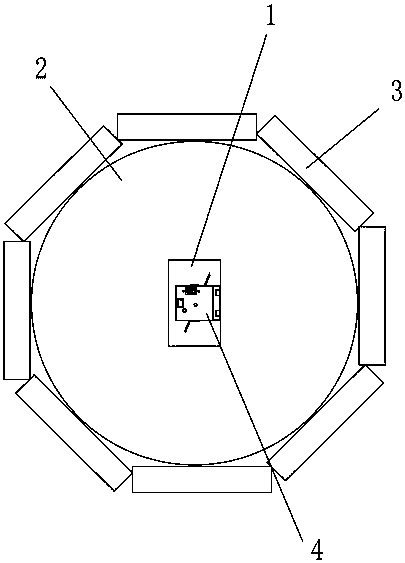
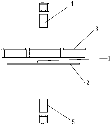
[0030] like Figure 1-3 Shown, the visual inspection method of the shallow scratch that originates from the quartz wafer surface of polishing of the present invention, comprises the following steps:
[0031] ...
PUM
 Abstract
Description
Claims
Application Information