Manufacturing method of embedded component circuit board and embedded component circuit board

A manufacturing method and circuit board technology, which is applied in the direction of assembling printed circuits with electrical components, printed circuits connected with non-printed electrical components, and printed circuit manufacturing. Issues that affect the reliability of the circuit board

Active Publication Date: 2018-04-20
GUANGZHOU FASTPRINT CIRCUIT TECH +2
View PDF14 Cites 1 Cited by
  • Summary
  • Abstract
  • Description
  • Claims
  • Application Information

AI Technical Summary

Problems solved by technology

[0002] With the miniaturization and multi-functionalization of electronic products, the requirements for electronic components and circuit boards are getting higher and higher. Mounting components on circuit boards can no longer meet the requirements.
[0003] In order to solve the above problems, a process of embedding electronic components inside the circuit board has emerged, which can effectively control the size of the finished circuit board. However, there are holes in the traditional circuit board embedded with electronic components, and other substances will remain in the cavity. , which affects the reliability of the circuit board when it is working

Method used


Image

  • Manufacturing method of embedded component circuit board and embedded component circuit board
  • Manufacturing method of embedded component circuit board and embedded component circuit board
  • Manufacturing method of embedded component circuit board and embedded component circuit board

Examples


Embodiment Construction

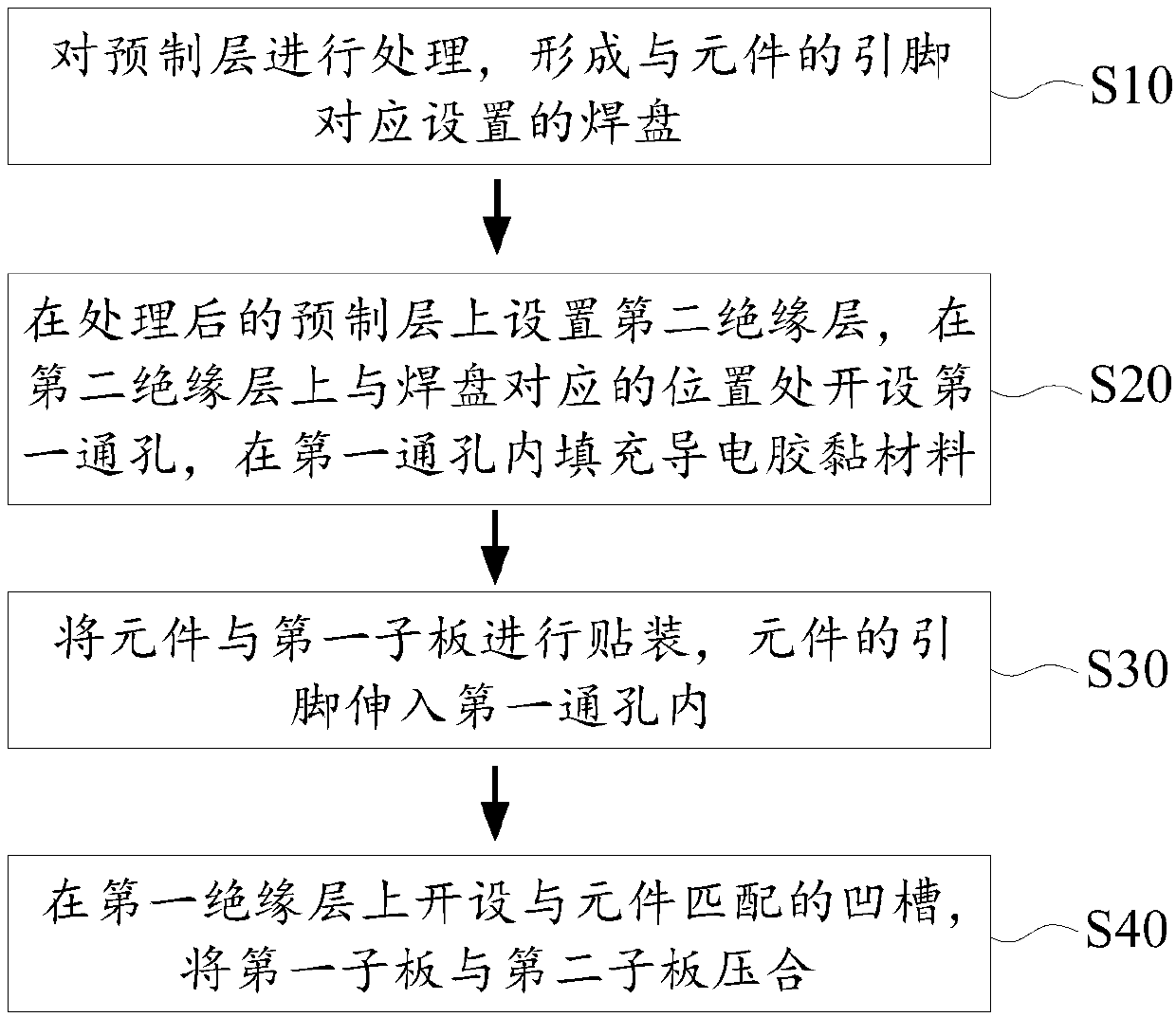
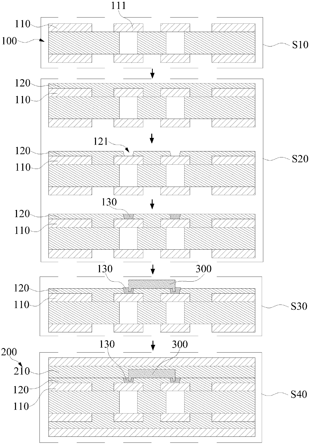
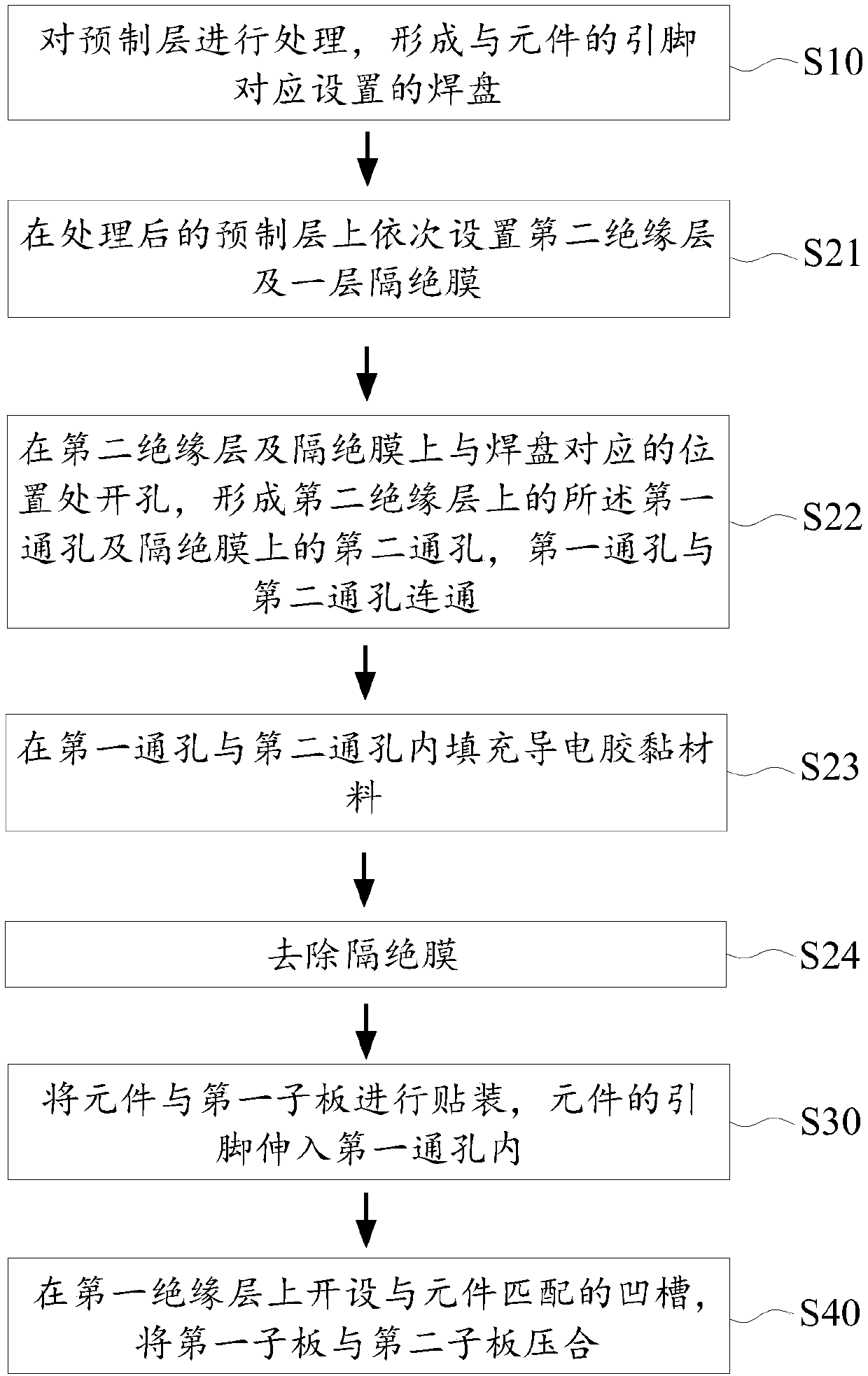
[0034] In order to facilitate the understanding of the present invention, the present invention will be described more fully below with reference to the associated drawings. Preferred embodiments of the invention are shown in the accompanying drawings. However, the present invention can be embodied in many different forms and is not limited to the embodiments described herein. On the contrary, the purpose of providing these embodiments is to make the disclosure of the present invention more thorough and comprehensive.

[0035] It should be noted that when an element is referred to as being “fixed” to another element, it can be directly on the other element or there can also be an intervening element. When an element is referred to as being "connected to" another element, it can be directly connected to the other element or intervening elements may also be present. The terms "vertical," "horizontal," "left," "right," and similar expressions are used herein for purposes of ill...


PUM


Abstract

The invention discloses a manufacturing method of an embedded component circuit board and the embedded component circuit board. The manufacturing method of the embedded component circuit board comprises the following steps that prefabricated layers are processed to form bonding pads arranged to correspond to pins of a component; a second insulating layer is arranged on the processed prefabricatedlayers, and first through holes are formed in the portions, corresponding to the bonding pads, of the second insulating layer and filled with a conducting adhesive material; the component is attachedto a first daughter board, and the pins of the component stretch into the first through holes; a groove matched with the component is formed in a first insulating layer; and the first daughter board and a second daughter board are pressed to be combined. According to the manufacturing method of the embedded component circuit board, the component can be fully attached to the second insulating layer, the component is closely matched with the first daughter board and the second daughter board, no hole exists, liquid is not likely to be retained in the circuit board, no influence is caused to workof the circuit board, and therefore the reliability of the manufactured circuit board is good.

Description

technical field [0001] The invention relates to the technical field of circuit board processing, in particular to a method for manufacturing a circuit board with embedded components and the circuit board with embedded components. Background technique [0002] With the miniaturization and multi-functionalization of electronic products, the requirements for electronic components and circuit boards are getting higher and higher, and installing components on circuit boards can no longer meet the requirements. [0003] In order to solve the above problems, a process of embedding electronic components inside the circuit board has emerged, which can effectively control the size of the finished circuit board. However, there are holes in the traditional circuit board embedded with electronic components, and other substances will remain in the cavity. , affecting the reliability of the circuit board when it is working. Contents of the invention [0004] Based on this, the present i...

Claims


Application Information

Patent Timeline
Patent Type & Authority Applications(China)
IPC IPC(8): H05K1/18H05K3/32
CPCH05K1/185H05K3/321H05K2203/0278
Inventor 吴森陈丽琴李艳国
Owner GUANGZHOU FASTPRINT CIRCUIT TECH
Why Eureka
Try Eureka