Light-emitting device and method of making the same

A technology for a light emitting device and a manufacturing method, which is applied to semiconductor devices, electrical components, circuits, etc., and can solve problems such as uneven color temperature of light emitted by a white light emitting diode structure

Active Publication Date: 2020-12-04
GENESIS PHOTONICS
View PDF4 Cites 0 Cited by
  • Summary
  • Abstract
  • Description
  • Claims
  • Application Information

AI Technical Summary

Problems solved by technology

The above phenomenon is also known as the yellow circle phenomenon, and this phenomenon causes the uneven color temperature of the light output of the white light emitting diode structure

Method used


Image

  • Light-emitting device and method of making the same
  • Light-emitting device and method of making the same
  • Light-emitting device and method of making the same

Examples


Embodiment Construction

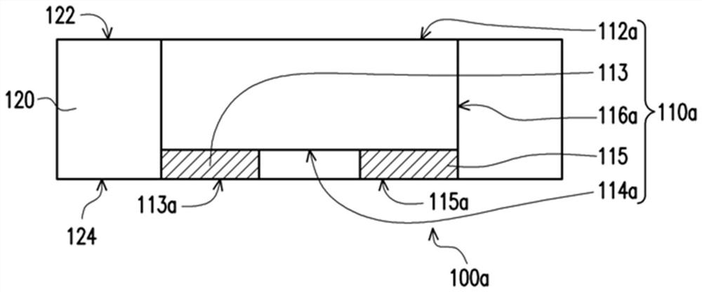
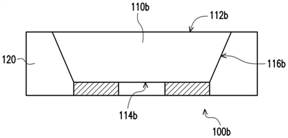
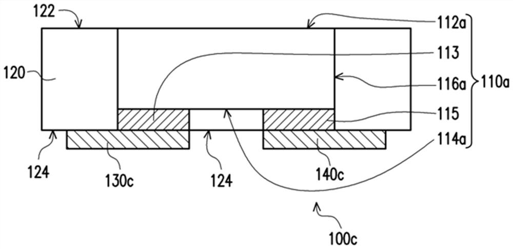
[0115] figure 1 A schematic diagram of a light emitting device according to an embodiment of the present invention is shown. Please refer to figure 1 , in this embodiment, the light emitting device 100a includes a light emitting unit 110a and a reflective protection member 120 . The light emitting unit 110a has an upper surface 112a and a lower surface 114a facing each other, a side surface 116a connecting the upper surface 112a and the lower surface 114a, and a first electrode pad 113 and a second electrode located on the lower surface 114a and separated from each other. Pad 115. The reflective protection member 120 covers the side surface 116a of the light emitting unit 110a and exposes at least part of the upper surface 112a and at least part of the first bottom surface 113a of the first electrode pad 113 and at least part of the second bottom surface of the second electrode pad 115. 115a.

[0116] More specifically, as figure 1 As shown, the upper surface 112a of the ...


PUM

PropertyMeasurementUnit
emission peakaaaaaaaaaa
particle diameteraaaaaaaaaa
thicknessaaaaaaaaaa

Abstract

A light-emitting device comprising: at least one light emitting unit, a wavelength converter layer, and a reflective protector.The light emitting unit has an upper surface and the lower surface of each other.The light emitting unit includes a two-electrode pad, and the two electrode pad is located in the lower surface.Wavelength conversion layer is disposed on the upper surface.The wavelength conversion layer includes a low concentration fluorescent layer and a high concentration of fluorescent collapsia.The high concentration fluorescent layer is located between the low concentration fluorescent layer and the light emitting unit.The reflective protector is covered with a light-emitting unit and a partially wavelength conversion layer, and at least the two electrode pad and low concentration fluorescent collapsy layer of the lateral unit are exposed.Width of high concentration fluorescent collaps H .Width of low concentration fluorescent layer is W L .The width of the light emitting unit is W E .The light emitting device is more satisfied with the following inequality.W E <W L W H <W L And 0.8 <W H / W E ≦ 1.2.Also, a method of fabricating a light-emitting device is also provided.

Description

technical field [0001] The present invention relates to a light-emitting device and a manufacturing method thereof, and in particular to a light-emitting device using a light-emitting diode as a light source and a manufacturing method thereof. Background technique [0002] In a general white light emitting diode structure, a layer of yellow phosphor is covered on the blue light emitting diode chip. The white light emission mechanism of the white light-emitting diode structure is to emit blue light through the blue light-emitting diode chip. Part of the blue light passes through the yellow phosphor on it and is converted into yellow light, and the yellow light is combined with other parts of the blue light to achieve white light. Effect. Since the blue light emitted by the blue light-emitting diode chip has a high degree of directivity, the blue light deviated from the optical axis at a large angle is weaker, while the blue light closer to the optical axis is stronger. Ther...

Claims


Application Information

Patent Timeline
Patent Type & Authority Patents(China)
IPC IPC(8): H01L33/20H01L33/46H01L33/50
CPCH01L33/20H01L33/46H01L33/505H01L2933/0025H01L2933/0041
Inventor 洪政暐杜隆琦张瑞夫曾春铭陈韵筑
Owner GENESIS PHOTONICS
Why Eureka
Try Eureka