Calibration wafer and method of manufacturing the same

A technology of wafer and deposition method, applied in semiconductor/solid-state device parts, semiconductor/solid-state device testing/measurement, semiconductor devices, etc., can solve the problems of melting point blasting, affecting the measurement accuracy of the machine, and achieve the effect of good thermal conductivity

Active Publication Date: 2019-11-26
ZING SEMICON CORP
View PDF4 Cites 0 Cited by
  • Summary
  • Abstract
  • Description
  • Claims
  • Application Information

AI Technical Summary

Problems solved by technology

[0005] The purpose of the present invention is to provide a calibration wafer and its manufacturing method to solve the problem that the calibration particles on the existing calibration wafer explode due to the high incident laser energy reaching its melting point, thereby affecting the measurement accuracy of the machine

Method used


Image

  • Calibration wafer and method of manufacturing the same
  • Calibration wafer and method of manufacturing the same
  • Calibration wafer and method of manufacturing the same

Examples


Embodiment 1

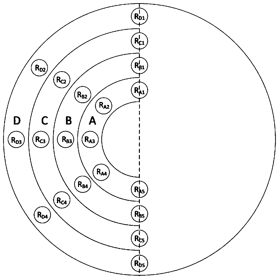
[0030] figure 2 Shown is a calibration wafer provided by the present invention, the calibration wafer includes a substrate wafer and calibration particles formed on the substrate wafer, the calibration particles are alumina particles, and the alumina particles pass through The deposition method deposits in one half of the surface of the substrate wafer.

[0031] In the first embodiment, the substrate wafer is divided into four scanning areas, which are the first scanning area A, the second scanning area B, the third scanning area C, and the fourth scanning area D. There are five groups of calibration particles in each scanning area.

[0032] Specifically, the substrate wafer is a conventional silicon wafer. Moreover, the shape of the substrate silicon wafer is circular. The first scanning area A, the second scanning area B, the third scanning area C, and the fourth scanning area D are all fan rings with the center of the circular substrate wafer as the center, and the The...

Embodiment 2

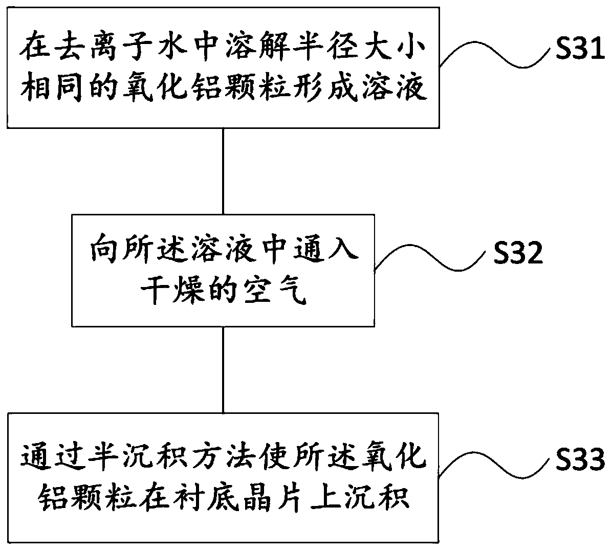
[0037] A method for manufacturing a calibration wafer, the schematic flow chart is as image 3 shown, including the following steps:

[0038] Step S31, dissolving alumina particles with the same radius in deionized water to form a solution;

[0039] Step S32, passing dry air into the solution;

[0040] Step S33, depositing the aluminum oxide particles on the substrate wafer by a semi-deposition method.

[0041] Specifically, the alumina particles are prepared by a sol-gel method, and the alumina particles are deposited on half of the surface of the substrate wafer by a semi-deposition method.

[0042] specific, Figure 4 for manufacturing figure 2The equipment for calibrating the wafer shown includes a syringe 41 for containing the solution; an air dryer 42 communicates with the syringe 41 through an air pipe, and feeds dry air into the solution in the syringe 41, and then injects dry air into the liner. While depositing the aluminum oxide particles on the bottom wafer, ...


PUM


Abstract

The invention provides a calibration wafer and a manufacturing method thereof. The calibration wafer comprises a substrate wafer and calibration particles formed on the substrate wafer for detecting the sensitivity of a stock. Alumina particles are used as calibration particles on the calibration wafer, the alumina particles have a good heat conduction coefficient, conduction of heat in a materialbody is facilitated, the alumina particles hardly cause volume expansion due to temperature rise, and the problem that explosion of calibration particles due to the rise of radiation temperature of high energy rays happens, and the stock measurement precision is influenced can thus be avoided.

Description

technical field [0001] The invention relates to the technical field of semiconductors, in particular to a calibration wafer and a manufacturing method thereof. Background technique [0002] With the increasing requirements of the integrated circuit industry and high-power device industry on the surface particle size of polished wafers and epitaxial wafers, how to detect nano-sized particles on the wafer surface, that is, to improve the sensitivity of the detection machine, has become a challenge for the detection industry. serious challenge. KLA-Tencor has successively developed a series of machines such as SP1, SP2, SP3 and SP5 by adjusting the incident light wavelength of the laser by using high-precision optical devices to detect the particle size of the wafer surface, and the sensitivity of these machines The corresponding improvement is due to the shortening of the incident laser wavelength. However, while the wavelength of the incident laser is shortened, the energy ...

Claims


Application Information

Patent Timeline
Patent Type & Authority Patents(China)
IPC IPC(8): H01L23/544
CPCH01L22/30
Inventor 王燕保罗·邦凡蒂刘源季文明
Owner ZING SEMICON CORP
Why Eureka
Try Eureka