Measurement method of word line resistance of 3D NAND

A word line resistance and measurement method technology, applied in the semiconductor field, can solve the problems of inability to measure word line resistance with a length of 6 mm, inability to uniformly grind target word lines, etc., and achieve the effect of facilitating smooth research and development and fast and accurate measurement

Active Publication Date: 2018-05-04
YANGTZE MEMORY TECH CO LTD
View PDF3 Cites 6 Cited by
  • Summary
  • Abstract
  • Description
  • Claims
  • Application Information

AI Technical Summary

Problems solved by technology

However, due to the limitation of the uniformity of sample grinding (single-layer word line thickness 0nm ~ 25nm, length 0mm ~ 6mm), it cannot be uniformly ground to the target word line, and the limitation of the measurement range of the nanoprobe (Nanoprober) (at m...

Method used


Image

  • Measurement method of word line resistance of 3D NAND
  • Measurement method of word line resistance of 3D NAND
  • Measurement method of word line resistance of 3D NAND

Examples


Embodiment Construction

[0022] Exemplary embodiments of the present disclosure will be described in more detail below with reference to the accompanying drawings. Although exemplary embodiments of the present disclosure are shown in the drawings, it should be understood that the present disclosure may be embodied in various forms and should not be limited by the embodiments set forth herein. Rather, these embodiments are provided for more thorough understanding of the present disclosure and to fully convey the scope of the present disclosure to those skilled in the art.

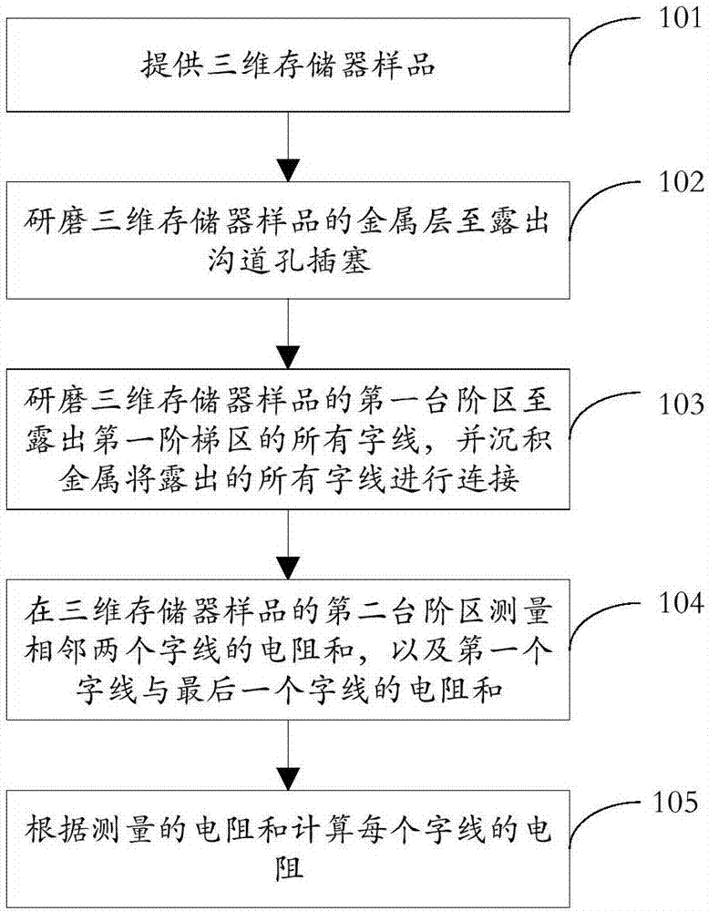
[0023] According to an embodiment of the present invention, a method for measuring the resistance of a three-dimensional memory word line is provided, such as figure 1 shown, including:

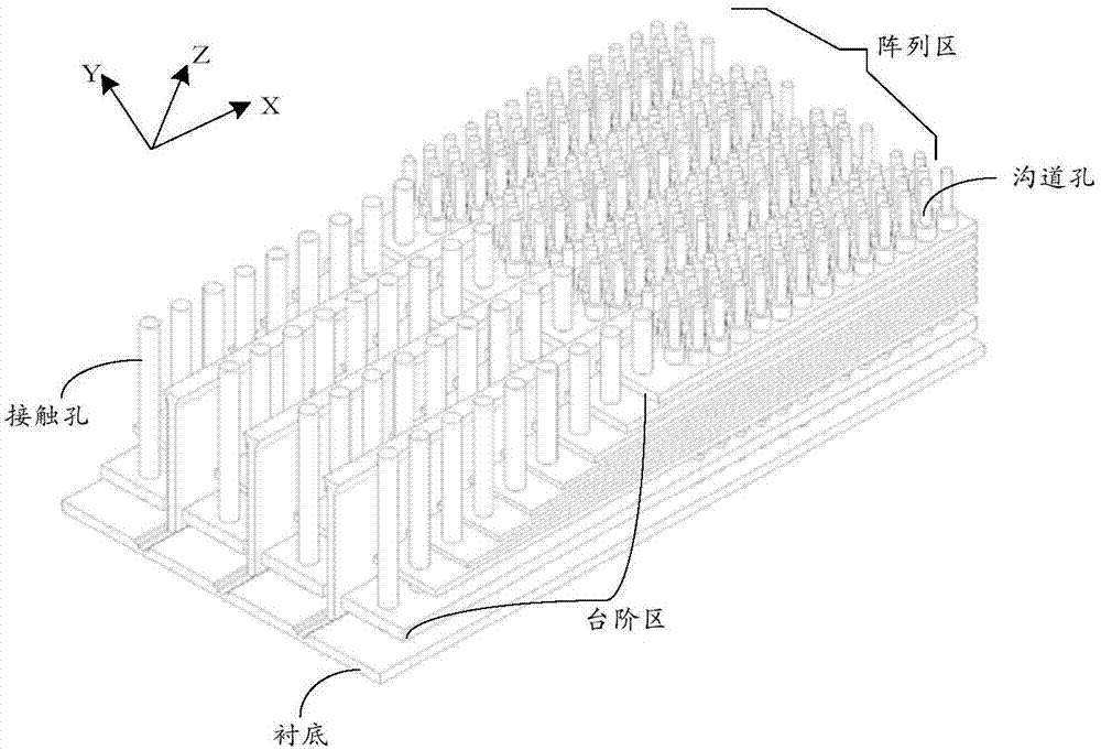
[0024] Provide a three-dimensional memory sample (there is no through hole (Via0) in the array area);

[0025] Grinding the metal layer of the three-dimensional memory sample to expose the channel hole plug;

[0026] Grinding the first step area...


PUM


Abstract

The invention discloses a measurement method of word line resistance of a 3D NAND, and belongs to the technical field of a semiconductor. The measurement method comprises the steps of providing a 3D NAND sample (there is no via in an array region); performing grinding on a metal layer of the 3D NAND sample until channel hole plugs appear; performing grinding on a first stage region of the 3D NANDsample until all word lines in the first stage region are exposed, and performing metal depositing to enable all exposed word lines to be connected; performing measurement on the sum of resistance oftwo adjacent word lines in a second stage region of the 3D NAND sample, and on the sum of resistance of the first word line and the last word line; and calculating the resistance of each word line according to the measured sum of resistance. By virtue of the measurement method, measurement of resistance of all word lines in the 3D NAND sample is realized quickly and accurately, thereby providing basis for electrical analysis of the 3D NAND and promoting smooth research and development of the 3D NAND product.

Description

technical field [0001] The invention relates to the technical field of semiconductors, in particular to a method for measuring the word line resistance of a three-dimensional memory. Background technique [0002] In the field of semiconductors, especially in the development stage of new products, various electrical data of chips are usually collected and analyzed. For three-dimensional memory (3D NAND), the word line (Word Line) resistance is an important measure of chip storage performance. parameter. For the measurement of block resistance, the two needle method or the Kelvin four-probe method is generally used to measure the sheet resistance of the conductor; for the word line width is small, the thickness is thin (0nm ~ 25nm), and the length is long (0mm ~ 6mm) , the measurement of the word line resistance of 3D NAND with high resistance generally adopts the method of two needles of the nanoprobe station (Nanoprober) to measure its resistance and ignores the contact res...

Claims


Application Information

Patent Timeline
IPC IPC(8): H01L21/66G01R27/02
CPCG01R27/02H01L22/14
Inventor 卢勤张顺勇汤光敏高慧敏
Owner YANGTZE MEMORY TECH CO LTD
Why Eureka
Try Eureka