Display back plate and manufacturing method and display device thereof

A technology for display backplanes and substrates, used in semiconductor/solid-state device manufacturing, electrical components, circuits, etc., can solve the problem of OLED display panel structure design to be improved, limited solubility and barrier height and hydrophobic properties, process window limitations, etc. question

Active Publication Date: 2018-05-04
BOE TECH GRP CO LTD
View PDF4 Cites 5 Cited by
  • Summary
  • Abstract
  • Description
  • Claims
  • Application Information

AI Technical Summary

Problems solved by technology

However, the solution-printed OLED is limited by the solubility of the material in the solvent, the height of the wall and the hydrophobicity, and cannot freely adjust the thickness of the functional layer like evaporation OLED, which leads to a significant limitation of the printing process window.
[0003] The red, green and blue (RGB) sub-pixels that print out OLEDs each have their own optimal light-emitting dipoles. If the RGB sub-pixels are set to the same second standing wave anti-node at the same time, it will cause red Light(R) process window is substantially limited
If the total thickness of the hole injection layer (HIL) and the hole transport layer (HTL) can be adjusted, the RGB sub-pixels can be arranged on the respective second standing wave anti-nodes, but the thickness of the HIL is not equal, and it will not be able to be processed once. The problem of film formation leads to complicated process
If the light-emitting dipole of the red sub-pixel is modified to the first standing wave antinode, the device leakage will be caused due to the thin film thickness of the overall device. Although the printing process window of the OLED structure display can be greatly enlarged, the overall red sub-pixel Device Thickness Excessive film thickness causes device leakage, which may affect the yield of the display
[0004] Therefore, the structural design of OLED display panels at this stage still needs to be improved.

Method used


Image

  • Display back plate and manufacturing method and display device thereof
  • Display back plate and manufacturing method and display device thereof
  • Display back plate and manufacturing method and display device thereof

Examples


Embodiment Construction

[0048] The following describes the embodiments of the present invention in detail, and those skilled in the art will understand that the following embodiments are intended to explain the present invention, and should not be regarded as limiting the present invention. Unless otherwise specified, in the following examples that do not explicitly describe specific techniques or conditions, those skilled in the art can carry out according to commonly used techniques or conditions in this field or according to product instructions.

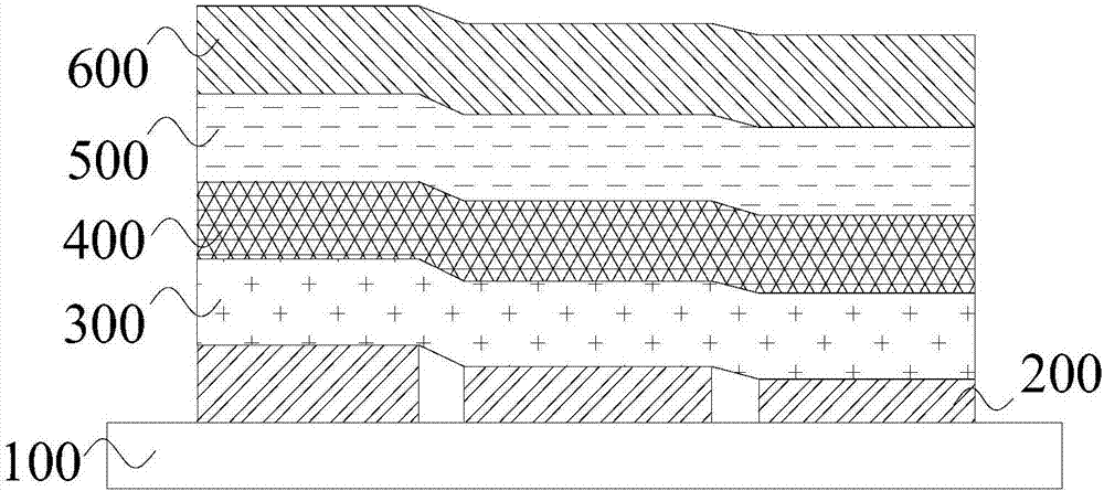
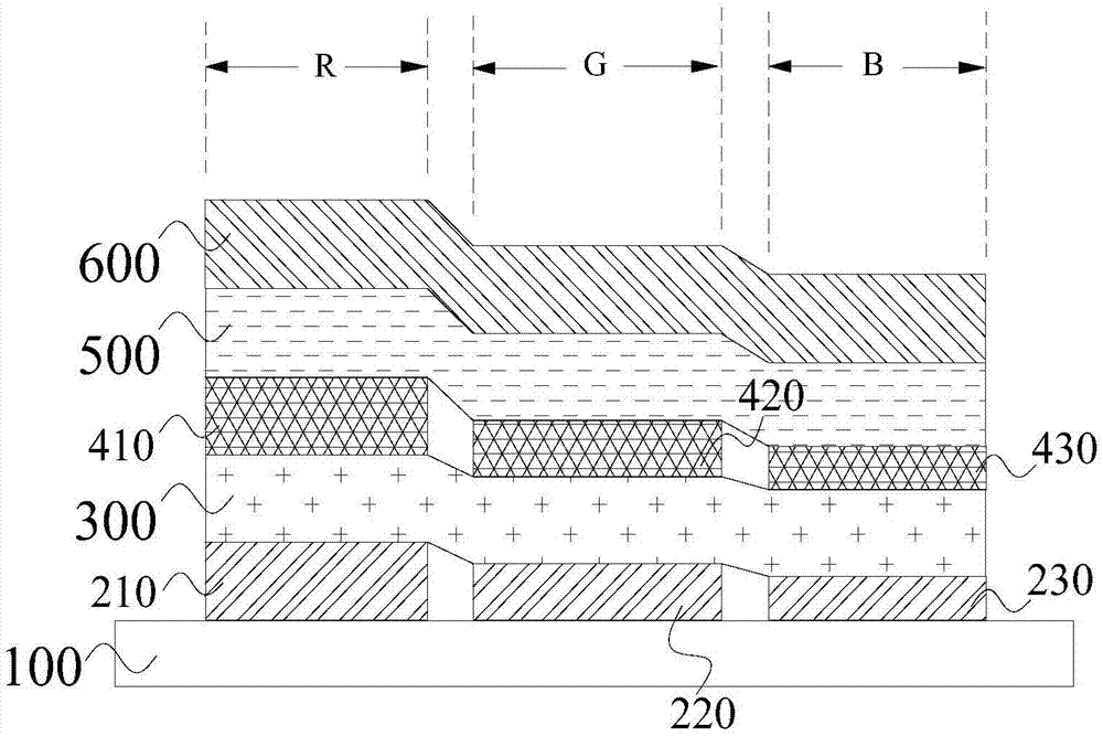
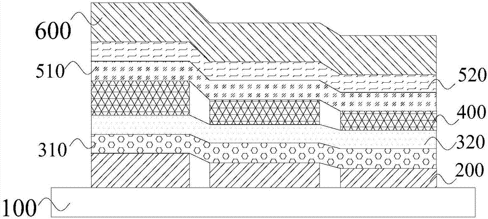
[0049] In one aspect of the invention, the invention provides a display backplane. refer to Figure 1~3 , to describe the display backplane of the present invention in detail.

[0050] According to an embodiment of the present invention, refer to figure 1 , the display backplane includes a plurality of pixel units distributed in an array, each pixel unit includes a plurality of sub-pixels, and each sub-pixel includes a substrate 100, a first electrode...


PUM


Abstract

The invention provides a display back plate and a manufacturing method and a display device thereof. The display back plate comprises a plurality of pixel units which are arranged in array, each pixelunit comprises a plurality of sub-pixels, each sub-pixel comprises a base plate, a first electrode, a first organic functional layer, an illuminating layer, a second organic functional layer and a second electrode, wherein illuminating colors of the plurality of sub-pixels are different, the thickness of the plurality of first electrodes of the plurality of sub-pixels is different, and the thickness of the first electrodes and the thickness of the first organic functional layers are used for making illuminating dipole moments of the sub-pixels located on second standing wave nodes of the first electrode side. According to the display back plate, the thickness of the first electrodes of different sub-pixels is different, so that the illuminating dipole moments of the different sub-pixels are installed on the second standing wave nodes of respective first electrode side, therefore the illuminating efficiency of the display back plate can be greatly improved, so that each other layer outside the illuminating layer in the display back plate is formed through a single process.

Description

technical field [0001] The present invention relates to the field of display technology, in particular, the present invention relates to a display backplane, a manufacturing method thereof, and a display device. Background technique [0002] At present, in order to reflect the characteristics of high material utilization and low manufacturing cost of organic light-emitting diodes (OLEDs), a variety of different sub-pixels need to be fabricated through multiple solution printing processes. However, solution-printed OLEDs are limited by the solubility of the material in the solvent, the height of the wall, and the hydrophobic properties, and cannot freely adjust the thickness of the functional layer like vapor-deposited OLEDs, resulting in a greatly limited printing process window. [0003] The red, green and blue (RGB) sub-pixels that print out OLEDs each have their own optimal light-emitting dipoles. If the RGB sub-pixels are set to the same second standing wave anti-node at...

Claims


Application Information

Patent Timeline
Patent Type & Authority Applications(China)
IPC IPC(8): H01L51/50H01L51/52H01L51/56H01L27/32
CPCH10K59/00H10K50/125H10K50/11H10K2101/10H10K50/805H10K71/00H10K59/35H10K50/85H10K2102/351H10K59/805H10K59/32
Inventor 闫光廖金龙杨栋芳
Owner BOE TECH GRP CO LTD
Why Eureka
Try Eureka