
Single-grain reinforced clock control circuit in programmable configuration logic block and control method thereof
A single-event reinforcement and configuration logic technology, which is applied to logic circuits with logic functions, etc., can solve problems such as user storage data errors, limited anti-single event flipping ability of programmable features, and user function interruption.
- Summary
- Abstract
- Description
- Claims
- Application Information
AI Technical Summary
Problems solved by technology
Method used
Image

Examples
Embodiment Construction
[0045] The present invention will be further described in detail below in conjunction with the accompanying drawings and specific embodiments.
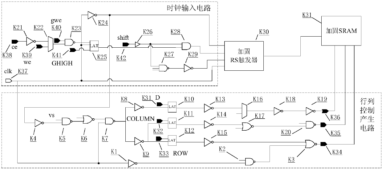
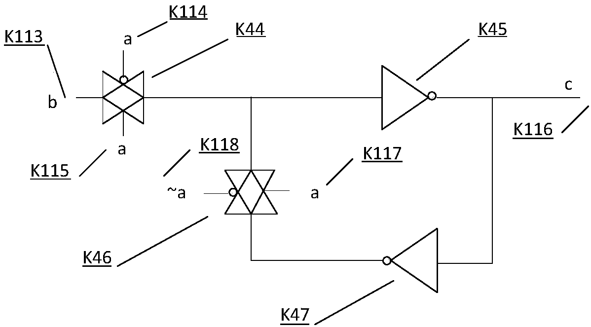
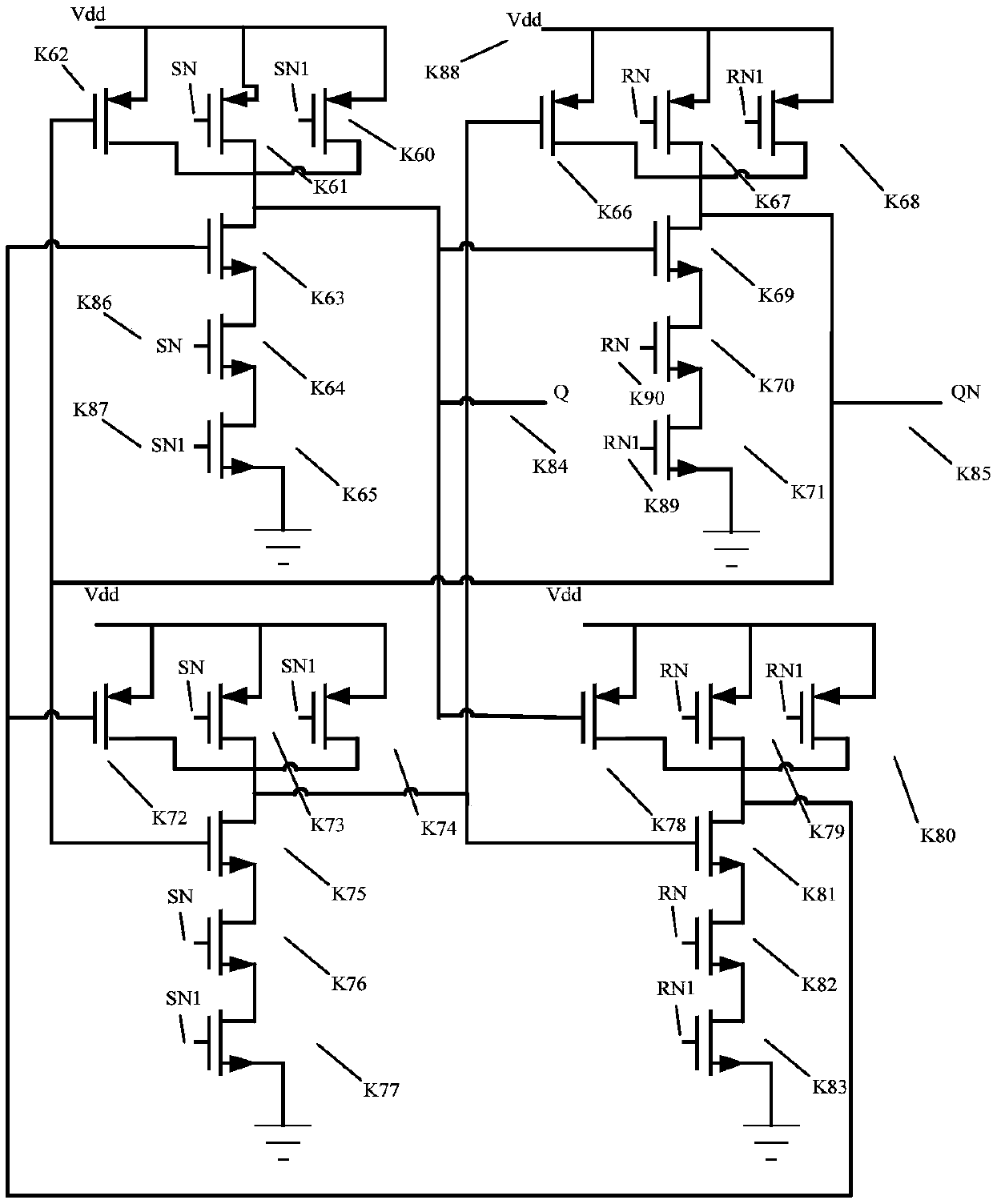
[0046] A single-particle reinforced clock control circuit and control method in a programmable configuration logic block of the present invention abandons the traditional clock control circuit, adopts timing and LAT structures to realize the latching and decoding of row, column and data signals, and realizes Synchronize the enable signal with the clock signal to generate a shifted overlapping clock to control the shifting of data; on this basis, the reinforced SRAM and the reinforced RS flip-flop design are used to realize the anti-single event hardening function of the user register, which improves the clock control circuit The ability to resist single instance flipping. The single event reinforcement index in the single event hardened clock control circuit of the present invention is 3 orders of magnitude higher than that of the tra...
PUM
 Abstract
Description
Claims
Application Information