Method for bonding semiconductor chips to landing wafer

A semiconductor and chip technology, applied in semiconductor devices, semiconductor/solid-state device manufacturing, electric solid-state devices, etc., can solve problems such as affecting the process and chip accuracy deviation

Pending Publication Date: 2018-05-22
INTERUNIVERSITAIR MICRO ELECTRONICS CENT (IMEC VZW) +1
View PDF4 Cites 1 Cited by
  • Summary
  • Abstract
  • Description
  • Claims
  • Application Information

AI Technical Summary

Problems solved by technology

This variation in liquid volume can lead to large deviations in

Method used


Image

  • Method for bonding semiconductor chips to landing wafer
  • Method for bonding semiconductor chips to landing wafer
  • Method for bonding semiconductor chips to landing wafer

Examples


Embodiment Construction

[0029] In the detailed description that follows, a surface is said to be "wettable" by an alignment fluid when a volume of fluid applied to the surface spreads readily across the surface. The liquid can be water or any other suitable alignment fluid. A surface that is wettable by water is said to be hydrophilic.

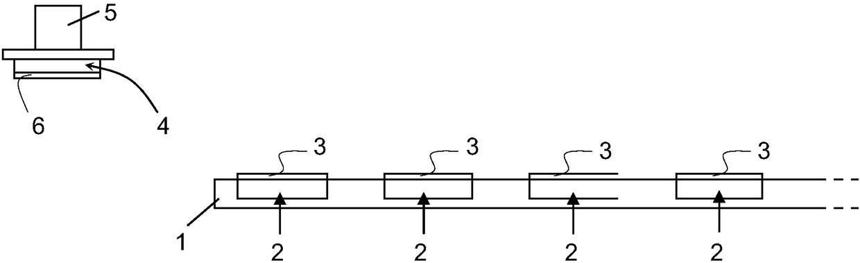
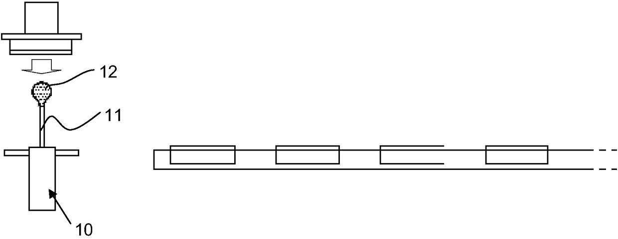
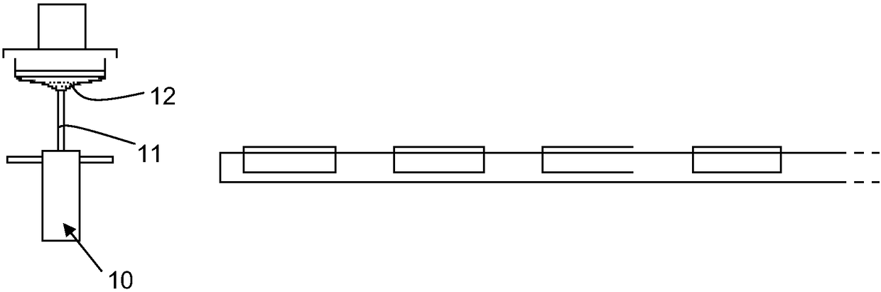
[0030] According to the method of the invention, the bonding surfaces of the bonding sites on chips and wafers can be at least partially wetted by a given alignment liquid, possibly made (more) wettable by plasma treatment, as known technology like that. However, in contrast to prior art methods, the method of the present invention includes the step of dispensing droplets of alignment fluid on the bonding surface of the chip before placing the chip on the wafer. Figures 1a to 1h The steps of a method according to a preferred embodiment are illustrated. A landed wafer 1 with a plurality of bonding locations 2 is provided ( Figure 1a ). These locations include an...


PUM


Abstract

The invention relates to a method for bonding chips to a landing wafer is disclosed. According to the method, certain volume of alignment liquid is dispensed on a wettable surface of the chip so as tobecome attached to the surface, after which the chip is moved towards the bonding site on the wafer, the bonding site equally being provided with a wettable surface. A liquid bridge is formed betweenthe chip and the bonding site on the substrate wafer, enabling self-alignment of the chip. Dispensing alignment liquid on the chip and not the wafer is advantageous in terms of mitigating unwanted evaporation of the liquid prior to bonding.

Description

technical field [0001] The present invention relates to the assembly of integrated circuit chips onto wafers. Wafers are also known as substrate wafers, landing wafers, carrier wafers or bottom wafers. The term "landing wafer" will be mainly used in this description. Background technique [0002] 3D integration of semiconductor chips (hereinafter also referred to as dies or integrated circuits) by bonding chips to a landing wafer or to a die or die stack previously bonded to the wafer is referred to as "die to wafer (D2W)" bonding or stacking. The technique involves the precise positioning of individual chips at predefined locations on the landing wafer, followed by collective bonding of the chips to the wafer. Accurate alignment of the chip can be facilitated by self-alignment of the chip to the landing wafer position by means of the use of an alignment fluid. Water is generally used for this purpose due to its high surface tension (72 mN / m) and low viscosity (1 cP at 2...

Claims


Application Information

Patent Timeline
IPC IPC(8): H01L21/68H01L21/56
CPCH01L21/56H01L21/68H01L2224/32245H01L24/75H01L24/83H01L2224/32145H01L2224/83143H01L2224/83002H01L2224/83896H01L24/94H01L2224/29186H01L24/29H01L24/32H01L2924/14H01L2224/80004H01L2224/80143H01L2224/97H01L2924/00012H01L2224/80001H01L2224/8002H01L2224/03318H01L2224/80355H01L2224/80908H01L2224/80986H01L2224/80169H01L2224/037H01L2224/03901
Inventor V·杜贝E·贝内G·卡普兹
Owner INTERUNIVERSITAIR MICRO ELECTRONICS CENT (IMEC VZW)
Why Eureka
Try Eureka