Photoelectronic device

A technology of optoelectronic devices and optical components, which is applied in the direction of instruments, optics, nonlinear optics, etc., can solve the problems of unfavorable network technology development, high production cost of optical equipment, and bulky devices, so as to reduce production costs, meet packaging requirements and The effect of low cost and good reliability

Active Publication Date: 2018-05-29
广东三石园科技有限公司
View PDF7 Cites 3 Cited by
  • Summary
  • Abstract
  • Description
  • Claims
  • Application Information

AI Technical Summary

Problems solved by technology

[0005] It can be seen that when the existing technology monitors the wavelength and power of the light beam, two optical splitters need to be installed, resulting in a bulky device and high production costs of optical equipment, which is not conducive to the development of network technology

Method used


Image

  • Photoelectronic device
  • Photoelectronic device
  • Photoelectronic device

Examples


no. 1 example

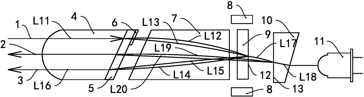
[0030] see figure 1 , The optoelectronic device of this embodiment has a fiber optic head 4, a beam splitting crystal 5, a half-wave plate 6, a self-focusing lens 7, a Faraday rotator 9, an angle wedge plate 10, and a photoelectric converter 11. Wherein, three optical fibers are arranged in the optical fiber head 4, which are optical fiber 1, optical fiber 2 and optical fiber 3, therefore, the optical fiber head 4 is a three-fiber optical fiber head, and the light beam input from the outside can enter the optoelectronic device through the optical fiber 1.

[0031] In this embodiment, the optical fiber 1, the optical fiber 2 and the optical fiber 3 all extend outward from the first end of the optical fiber head 4, the light splitting crystal 5 is closely attached to the second end of the optical fiber head 4, and the half-wave plate 6 is close to the light splitting crystal 5 away from the side of the fiber optic head 4. In this embodiment, the half-wave plate 6 is only arran...

no. 2 example

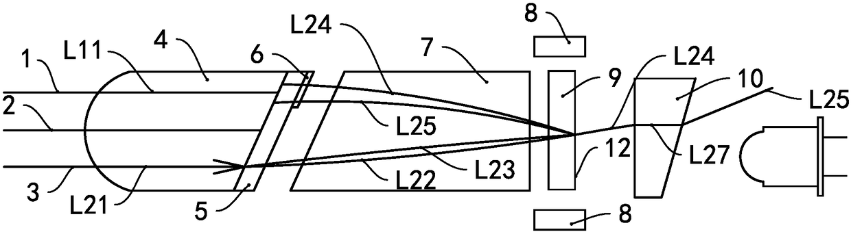
[0051] see Figure 4 , The optoelectronic device of this embodiment has a fiber optic head 24, a beam splitting crystal 25, a half-wave plate 26, a Faraday rotator 28, a self-focusing lens 29, an angle wedge plate 30, and a photoelectric converter 31. Wherein, three optical fibers are arranged in the optical fiber head 24 , namely the optical fiber 21 , the optical fiber 22 and the optical fiber 23 , and the light beam input from the outside can enter the optoelectronic device through the optical fiber 21 .

[0052] In this embodiment, the optical fiber 21, the optical fiber 22 and the optical fiber 23 all extend outward from the first end of the optical fiber head 24, the light splitting crystal 25 is close to the second end of the optical fiber head 24, and the half-wave plate 26 is close to the light splitting crystal. 25 away from the side of the fiber head 24. In this embodiment, the half-wave plate 26 is only arranged on the optical path of the optical fiber 21 .

[00...

no. 3 example

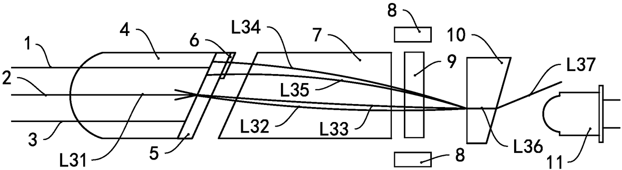
[0068] Optoelectronic Devices Optoelectronic Devices Optoelectronic Devices See Figure 7 , In this embodiment, the optoelectronic device has a fiber optic head 64, a beam splitting crystal 65, a half-wave plate 66, a self-focusing lens 67, a Faraday rotator 69, an angle wedge plate 70, and a photoelectric converter 71. Wherein, the optical fiber head 64 is provided with three optical fibers, namely the optical fiber 61, the optical fiber 62 and the optical fiber 63. Therefore, the optical fiber head 64 is a three-fiber optical fiber head, and the light beam input from the outside can enter the optoelectronic device through the optical fiber 61.

[0069] In this embodiment, the optical fiber 61, the optical fiber 62 and the optical fiber 63 all extend outward from the first end of the optical fiber head 64, the light splitting crystal 65 is attached to the second end of the optical fiber head 64, and the half-wave plate 66 is attached to the second end of the optical fiber head...


PUM


Abstract

The invention provides a photoelectronic device. The photoelectronic device comprises an optical fiber head. Three optical fibers are arranged in the optical fiber head, and extend to the outside of the first end of the optical fiber head. An analyzing crystal is arranged at the second end of the optical fiber head. A half wave plate is arranged on one side, away from the optical fiber head, of the analyzing crystal. A focusing optical rotation component is arranged on one side of the second end of the optical fiber head, and comprises a self-focusing lens and a Faraday optical rotation device. A first reflecting and transmitting film is arranged on one side, away from the optical fiber head, of the focusing optical rotation component. The reflectivity of the first reflecting and transmitting film is much smaller than the transmittivity thereof. A wedge angle sheet is arranged on one side, away from the optical fiber head, of the focusing optical rotation component. A photoelectronic converter is arranged on one side, away from the focusing optical rotation component, of the wedge angle sheet. A second reflecting and transmitting film is arranged on one side, close to the focusingoptical rotation component, of the wedge angle sheet. The reflectivity of the second reflecting and transmitting film is much larger than the transmittivity thereof. The photoelectronic device has theadvantages that miniaturization of an optical mixing device can be realized, and the optical mixing device can have optical isolation and photoelectronic detection functions.

Description

technical field [0001] The invention relates to an optical device, in particular to an optoelectronic device with small volume and integrated optical isolation function. Background technique [0002] With the development of network communication, the data transmission speed of the optical fiber network is getting faster and faster, and the requirement for the capacity of the optical fiber network is also getting higher and higher. The existing optical fiber network transmission system uses a large number of various optical devices, such as isolators, optical splitters, depolarizers, etc. With the development of technology, various devices need to be used comprehensively to achieve the required functions. Therefore, the existing Fiber optic networks make extensive use of various optical hybrid devices. [0003] Existing optical hybrid devices are mainly devices with optical fibers at both ends. This is the most common optical device. The total length of this optical hybrid d...

Claims


Application Information

Patent Timeline
Patent Type & Authority Applications(China)
IPC IPC(8): G02F1/095
CPCG02F1/0955
Inventor 郭宗海杨立
Owner 广东三石园科技有限公司
Why Eureka
Try Eureka