Resistance-variable type non-volatile memory and operating method thereof

A non-volatile memory technology, applied in static memory, read-only memory, information storage, etc., can solve the problem of deterioration of flat panel display aperture ratio, resolution performance index, hindering memory size reduction and storage density improvement, unit size Large and other problems, to achieve the effect of compact structure, low power consumption and fast working speed

Active Publication Date: 2018-05-29
SOUTHEAST UNIV
View PDF3 Cites 0 Cited by
  • Summary
  • Abstract
  • Description
  • Claims
  • Application Information

AI Technical Summary

Problems solved by technology

Therefore, compared with charge-type memory, InGaZnO resistive memory has the disadvantage of large cell size, which not only seriously hinders the r

Method used


Image

  • Resistance-variable type non-volatile memory and operating method thereof
  • Resistance-variable type non-volatile memory and operating method thereof

Examples


Example Embodiment

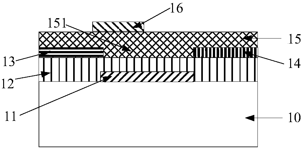
[0021] Implementation Mode 1

[0022] like figure 1 As shown, a resistive nonvolatile memory is composed of a bottom-gate bottom-contact thin film transistor and a resistive memory. The resistive memory includes a top gate 16, an InGaZnO semiconductor layer 15, a source 13 and a drain 14, and the top gate 16 is arranged on the InGaZnO semiconductor layer 15, the convex part below the InGaZnO semiconductor layer 15 is a channel 151, and the source 13 and the drain 14 are respectively arranged on both sides of the channel 151, and the top gate 16 overlaps with the source 13. The length of the overlapping region is 0.5 μm to 5 μm, the vertical distance between the top gate 16 and the source 13 and the drain 14 is 10 nm to 50 nm, the length of the channel 151 below the InGaZnO semiconductor layer is less than 10 m, and the channel of the InGaZnO semiconductor layer 15 The length of the track 151 is 1-5 times the length of the overlapping region of the top gate 16 and the source 1...

Example Embodiment

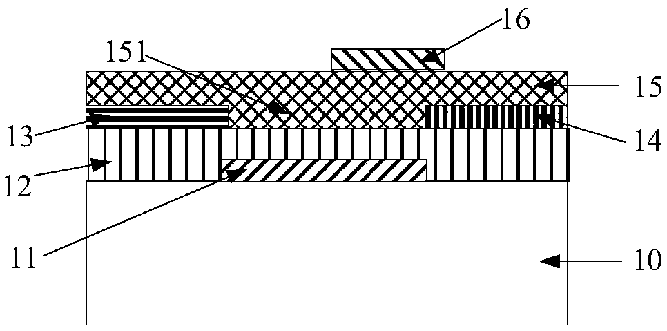
[0030] Implementation Mode Two

[0031] like figure 2 As shown, a resistive nonvolatile memory is composed of a bottom-gate bottom-contact thin film transistor and a resistive memory. The resistive memory includes a top gate 16, an InGaZnO semiconductor layer 15, a source 13 and a drain 14, and the top gate 16 is arranged on the InGaZnO semiconductor layer 15, the convex part below the InGaZnO semiconductor layer 15 is a channel 151, and the source electrode 13 and the drain electrode 14 are respectively arranged on both sides of the channel 151, and the top gate 16 overlaps with the drain electrode 14. The length of the overlapping region is 0.5 μm to 5 μm, the vertical distance between the top gate 16 and the source 13 and the drain 14 is 10 nm to 50 nm, the length of the channel 151 below the InGaZnO semiconductor layer is less than 10 m, and the channel of the InGaZnO semiconductor layer 15 The length of the track 151 is 1-5 times the length of the overlapping region of ...


PUM

PropertyMeasurementUnit
Lengthaaaaaaaaaa

Abstract

The present invention discloses a resistance-variable type non-volatile memory and an operating method thereof. The resistive variable type non-volatile memory includes a bottom gate bottom contact type thin film transistor and a resistance-variable type memory, wherein the bottom gate bottom contact type thin film transistor is composed of a bottom gate, a gate oxide layer, a source, a drain, and a semiconductor layer, and the resistance-variable type memory is composed of the overlapping portion of a top gate and the source or the drain; the top gate is disposed on the semiconductor layer;the source and the drain are disposed at two sides of the lower part of the semiconductor layer; a portion of the semiconductor layer, which is located between the source and the drain, is called a channel; the bottom of the channel contacts with the gate oxide layer; and the bottom gate is arranged at the lower part of the gate oxide layer. The semiconductor resistance-variable type memory provided by the present invention has the advantages of compact structure, small size and the like compared with a conventional resistance-variable type memory. The operating method based on the resistance-variable type memory can perform efficient storage.

Description

technical field [0001] The invention relates to a nonvolatile memory and an operation method for realizing information storage and acquisition by the nonvolatile memory, in particular to a resistive nonvolatile memory and an operation method thereof. Background technique [0002] Flat panel displays are widely used in various electronic devices such as TVs, computers, and mobile phones, which have greatly changed people's lifestyles. At present, the flat panel display industry has become a pivotal industry in my country's national economy. Thin-film transistors and non-volatile memory are the basic devices that constitute flat panel displays. The former mainly plays the role of switching and driving, and the latter mainly plays the role of information storage. For thin film transistors and nonvolatile memories, their performance is closely related to the material of the semiconductor layer. Traditional amorphous silicon semiconductor materials have good uniformity but low m...

Claims


Application Information

Patent Timeline
IPC IPC(8): H01L27/115G11C16/02
CPCG11C16/02H10B69/00
Inventor 黄晓东李帆黄见秋
Owner SOUTHEAST UNIV
Why Eureka
Try Eureka