Large-aperture acousto-optical tunable filter

A technology of large aperture and optical filter, which is applied in the direction of instruments, optics, nonlinear optics, etc., can solve the problems of not being able to withstand large driving electric power, difficulty in making the optical aperture large, and poor welding quality, etc., to achieve uniform diffraction efficiency Sexual problems, improve reliability, and improve the effect of firmness

CN108107610AActive Publication Date: 2018-06-01CHINA ELECTRONICS TECH GRP NO 26 RES INST
5 Cites 2 Cited by

Patent Information

Authority / Receiving Office
CN · China
Current Assignee / Owner
Publication Date
2018-06-01

Smart Images

  • Figure 1
    Figure 1
  • Figure 2
    Figure 2
Patent Text Reader

Abstract

The invention discloses a large-aperture acousto-optical tunable filter which comprises an acousto-optical medium, an energy converter and five welding layers. The energy converter is connected with the acousto-optical medium through the welding layers, a bottoming layer I, a transition layer I, a bonding layer, a transition layer II and a bottoming layer II are sequentially arranged from the acousto-optical medium to the energy converter, a surface electrode is plated on the energy converter, both the bottoming layer I and the bottoming layer II are titanium film layers, both the transition layer I and the transition layer II are copper film layers, and the bonding layer is a tin silver indium alloy layer. During manufacture, evaporation sources are arranged on two sides of the energy converter and the acousto-optical medium and evaporate bonding layer materials for the energy converter and the acousto-optical medium to obtain large-area uniform thickness bonding layer films, and thebonding layer films simultaneously cover the copper film layers of the energy converter and the acousto-optical medium. The acousto-optical tunable filter solves the problems that the optical apertureof an existing acousto-optical tunable filter is difficultly made large, welding quality is not good enough and cannot bear high driving electric power and the like.
Need to check novelty before this filing date? Find Prior Art

Description

technical field

[0001] The invention relates to an acousto-optic device, in particular to an acousto-optic tunable filter with a larger optical aperture. Background technique

[0002] Hyperspectral imaging technology based on acousto-optic tunable filter is one of the most effective technical means for international military reconnaissance. It can quickly find targets that cannot be identified by conventional means, and is of great significance in anti-stealth / camouflage, detailed battlefield inspection, target search and accurate identification, etc. It can be widely used in hyperspectral and hyperspectral imaging warning and reconnaissance systems such as aircraft missiles Early warning, battlefield reconnaissance, mine detection, offshore detection, anti-submarine reconnaissance and evaluation of ammunition damage effects.

[0003] The acousto-optic tunable filter is a key component in the acousto-optic hyperspectral imaging system. The larger the optical aperture, the s...

Examples

Embodiment Construction

[0019] The above-mentioned structural improvements of the present invention will be described in detail below with reference to the accompanying drawings and specific embodiments.

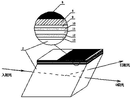
[0020] see figure 1 , as can be seen from the figure, the large aperture acousto-optic tunable filter of the present invention is mainly composed of acousto-optic medium 2, transducer 5, surface electrode 8, titanium film I9, copper film I10, bonding layer 11, copper It is composed of film II12 and titanium film II13.

[0021] Between the acousto-optic medium 2 and the transducer 5 is a welding layer. The welding layer is composed of titanium film I9 (priming layer), copper film I10 (transition layer), bonding layer 11 (tin-silver-indium alloy layer), copper film II12 (transition layer) and titanium film II13 (priming layer), the thickness of titanium film I9 and titanium film II13 is 10nm-15nm, the thickness of copper film I10 and copper film II12 is 200nm-250nm, the thickness of bonding layer 11...