Imaging device
An imaging device and pixel technology, which is applied in the direction of electric solid-state devices, semiconductor devices, instruments, etc., can solve problems such as image quality degradation, insufficient shading, and error signals, and achieve the effect of reducing image quality degradation
- Summary
- Abstract
- Description
- Claims
- Application Information
AI Technical Summary
Problems solved by technology
Method used
Image

Examples
no. 1 example
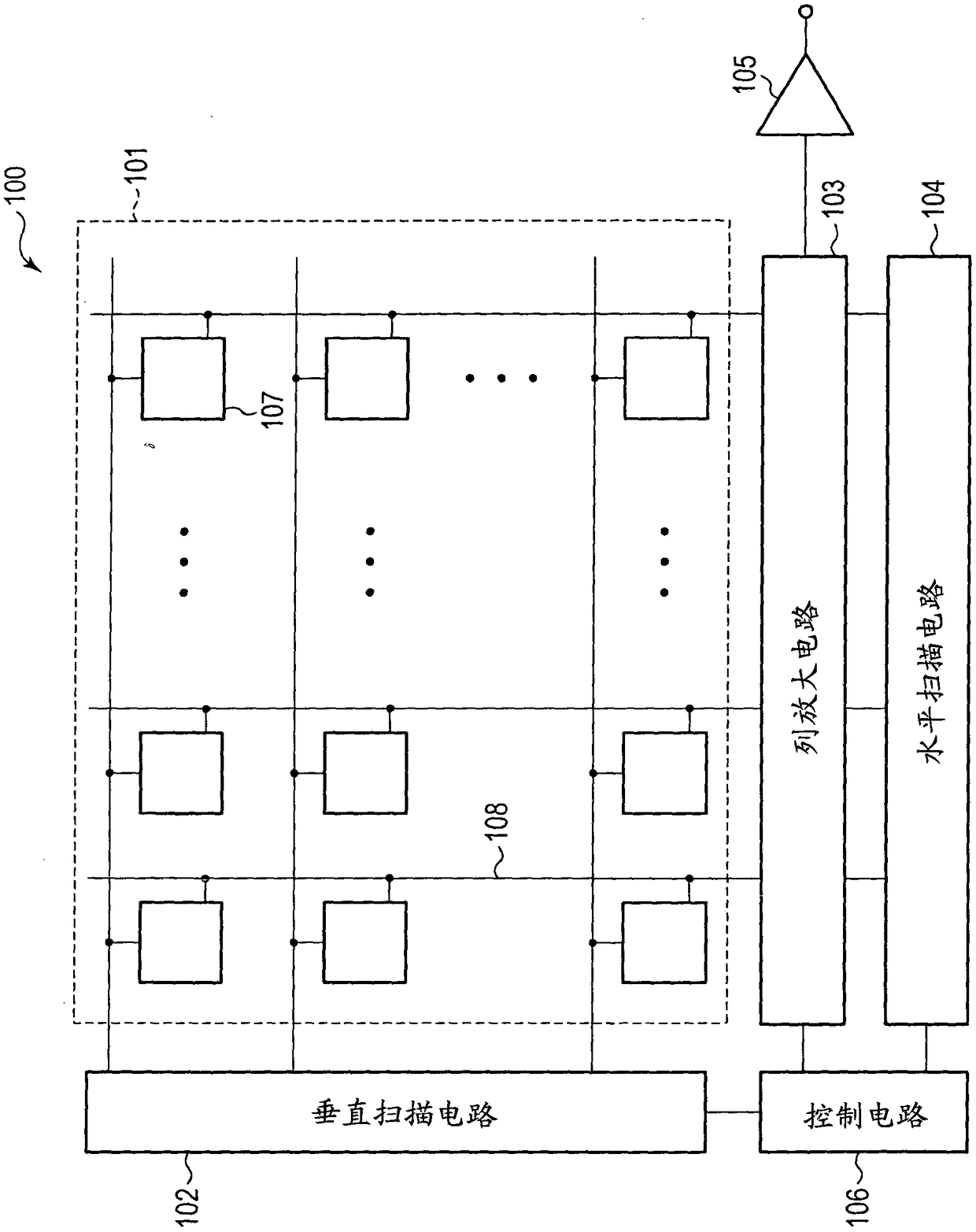
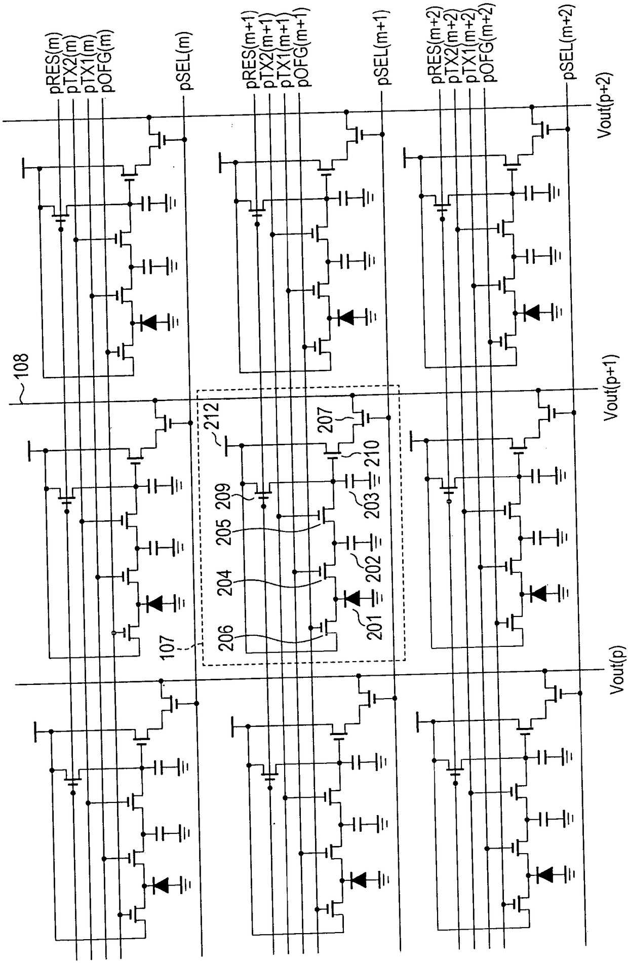
[0021] figure 1 is a block diagram showing the overall configuration of the imaging device 100 according to the present embodiment. The imaging device 100 has a pixel array 101 , a vertical scanning circuit 102 , a column amplification circuit 103 , a horizontal scanning circuit 104 , an output circuit 105 and a control circuit 106 . The imaging device 100 is a semiconductor device formed on a semiconductor substrate such as a silicon substrate, and is a CMOS image sensor in this embodiment. The pixel array 101 has a plurality of pixels 107 arranged two-dimensionally including a plurality of rows and a plurality of columns on a semiconductor substrate. The vertical scanning circuit 102 supplies a plurality of control signals for controlling a plurality of transistors included in the pixel 107 to be turned on (conducting state) or turned off (non-conducting state). A column signal line 108 is provided on each column of the pixels 107, and a signal from the pixel 107 is read o...
no. 2 example
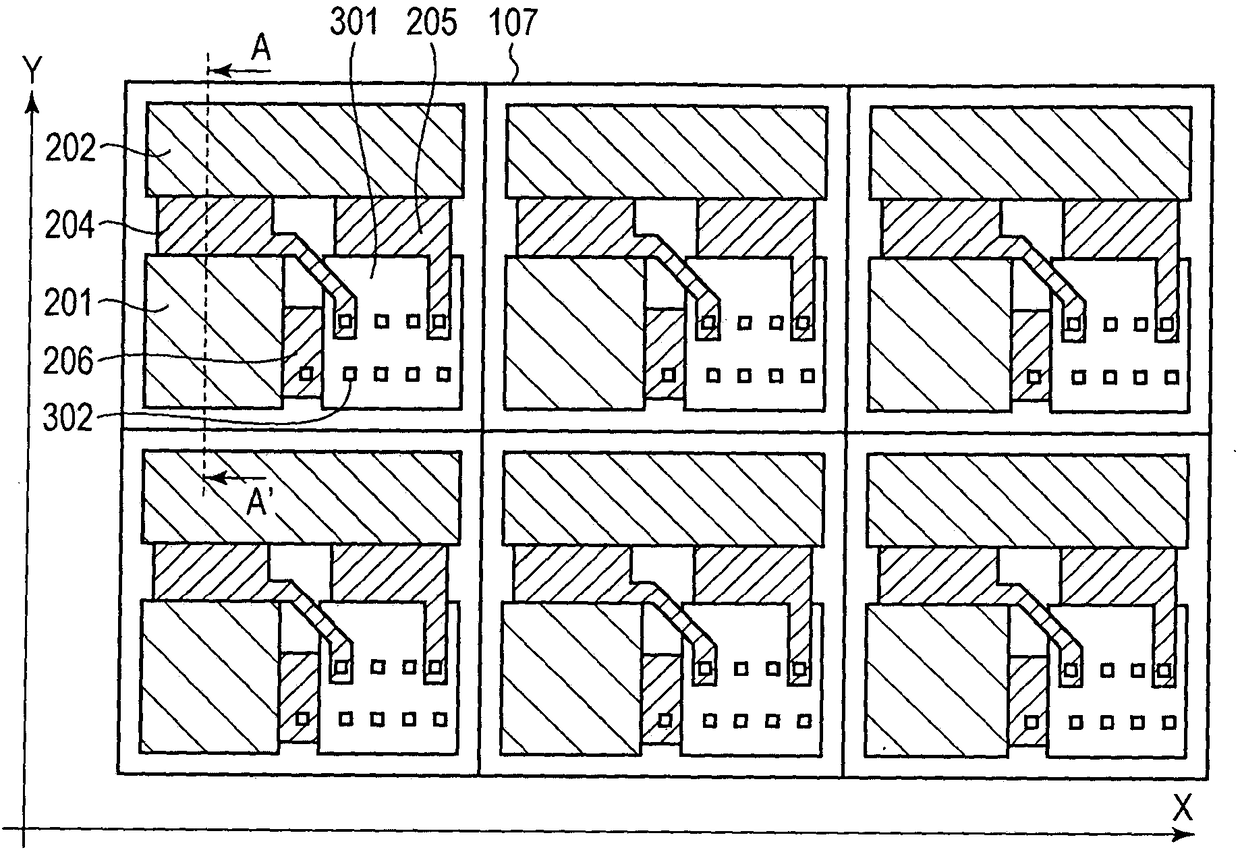
[0039] Figure 6A and Figure 6B is a plan view of the pixel 107 of the imaging device 100 according to the second embodiment. Figure 6A is a plan view schematically showing a pattern near the surface of the semiconductor substrate in a plan view in a direction perpendicular to the semiconductor substrate, Figure 6B is a plan view mainly schematically showing the pattern of the light shielding portion 303 formed over the semiconductor substrate. In the description of the present embodiment, detailed descriptions of features common to the first embodiment are omitted. and, in Figure 6A and Figure 6B in, with Figure 3A and Figure 3B Features with the same functions in etc. are denoted by the same reference numerals, and descriptions of their functions may be omitted.
[0040] Such as Figure 6AAs shown, the present embodiment differs from the first embodiment in that two first transfer transistors 204 , two second transfer transistors 205 and two charge holding uni...
no. 3 example
[0044] Figure 7A and Figure 7B is a plan view of the pixel 107 of the imaging device 100 according to the third embodiment. Figure 7A is a plan view schematically showing a pattern near the surface of the semiconductor substrate in a plan view in a direction perpendicular to the semiconductor substrate, Figure 7B is a plan view mainly schematically showing the pattern of the light shielding portion 303 formed over the semiconductor substrate. In the description of the present embodiment, detailed descriptions of features common to those of the first embodiment or the second embodiment are omitted. and, in Figure 7A and Figure 7B in, with Figure 3A and Figure 3B Features with the same functions in etc. are denoted by the same reference numerals, and descriptions of their functions may be omitted.
[0045] Such as Figure 7A As shown, in this embodiment, similar to the second embodiment, two first transfer transistors 204 , two second transfer transistors 205 and...
PUM
 Abstract
Description
Claims
Application Information
 - Generate Ideas
- Intellectual Property
- Life Sciences
- Materials
- Tech Scout
- Unparalleled Data Quality
- Higher Quality Content
- 60% Fewer Hallucinations
Browse by: Latest US Patents, China's latest patents, Technical Efficacy Thesaurus, Application Domain, Technology Topic, Popular Technical Reports.
© 2025 PatSnap. All rights reserved.Legal|Privacy policy|Modern Slavery Act Transparency Statement|Sitemap|About US| Contact US: help@patsnap.com