Liquid crystal display device

a liquid crystal display and display panel technology, applied in the field of display devices, can solve the problems of reducing the thickness of the liquid crystal display panel, reducing the manufacturing yield rate, and difficult to acquire such standardized glass substrates from the market, so as to improve the design aesthetics and lessen the degradation of image quality

Active Publication Date: 2011-09-13
PANASONIC INTELLECTUAL PROPERTY CORP OF AMERICA +1
View PDF9 Cites 20 Cited by
  • Summary
  • Abstract
  • Description
  • Claims
  • Application Information

AI Technical Summary

Benefits of technology

[0012]The present invention has been made in view of the above-mentioned circumstances, and it is therefore an object of the present invention to prevent the deterioration of a displayed image that results from the presence of an attached face plate and, at the same time, to solve the problem of the adhesion between a liquid crystal display panel and a face plate being affected by a graphic pattern that is drawn by printing or other measures along the perimeter of the face plate for the purpose of attaining improved design aesthetics.
[0023]The present invention makes it possible to bond the face plate made of glass to the liquid crystal display panel while considerably lessening image quality degradation that is caused by reflection at the interface between the face plate and the liquid crystal display panel. The present invention also ensures that the adhesion between the face plate and the liquid crystal display panel is steady despite the presence of the frame formed along the perimeter of the face plate by printing for the purpose of attaining improved design aesthetics.
[0024]In addition, using the three-layer structure pressure-sensitive adhesive member that has the first pressure-sensitive adhesive member, the base, and the second pressure-sensitive adhesive member as a pressure-sensitive adhesive material for bonding the face plate to the liquid crystal display panel, the present invention makes it possible to salvage and reuse the liquid crystal display panel, the face plate, and other components even when a defect in bonding between the face plate and the liquid crystal display panel calls for repairs.

Problems solved by technology

It is difficult to acquire such standardized glass substrate from a market.
Further, an extremely thin glass substrate gives rise to drawbacks on mechanical strength, deflection, or the like in manufacturing steps thereof thus lowering a manufacturing yield rate.
The reduction of the thickness of the liquid crystal display panel gives rise to a drawback on mechanical strength.
That is, there exists a risk that the liquid crystal display panel is broken when mechanical pressure is applied to a display screen of the liquid crystal display panel.
This, however, causes a different problem in a structure illustrated in FIG. 16 by degrading the quality of a displayed image as is described later.
The related art illustrated in FIG. 16 gives rise to a drawback that an image appears as a duplicate image. FIG. 16 is a view describing the drawback by taking a reflective liquid crystal display panel as an example.
The phenomenon which makes the image appear as a duplicate image deteriorates image quality.

Method used


Image

  • Liquid crystal display device
  • Liquid crystal display device
  • Liquid crystal display device

Examples


first embodiment

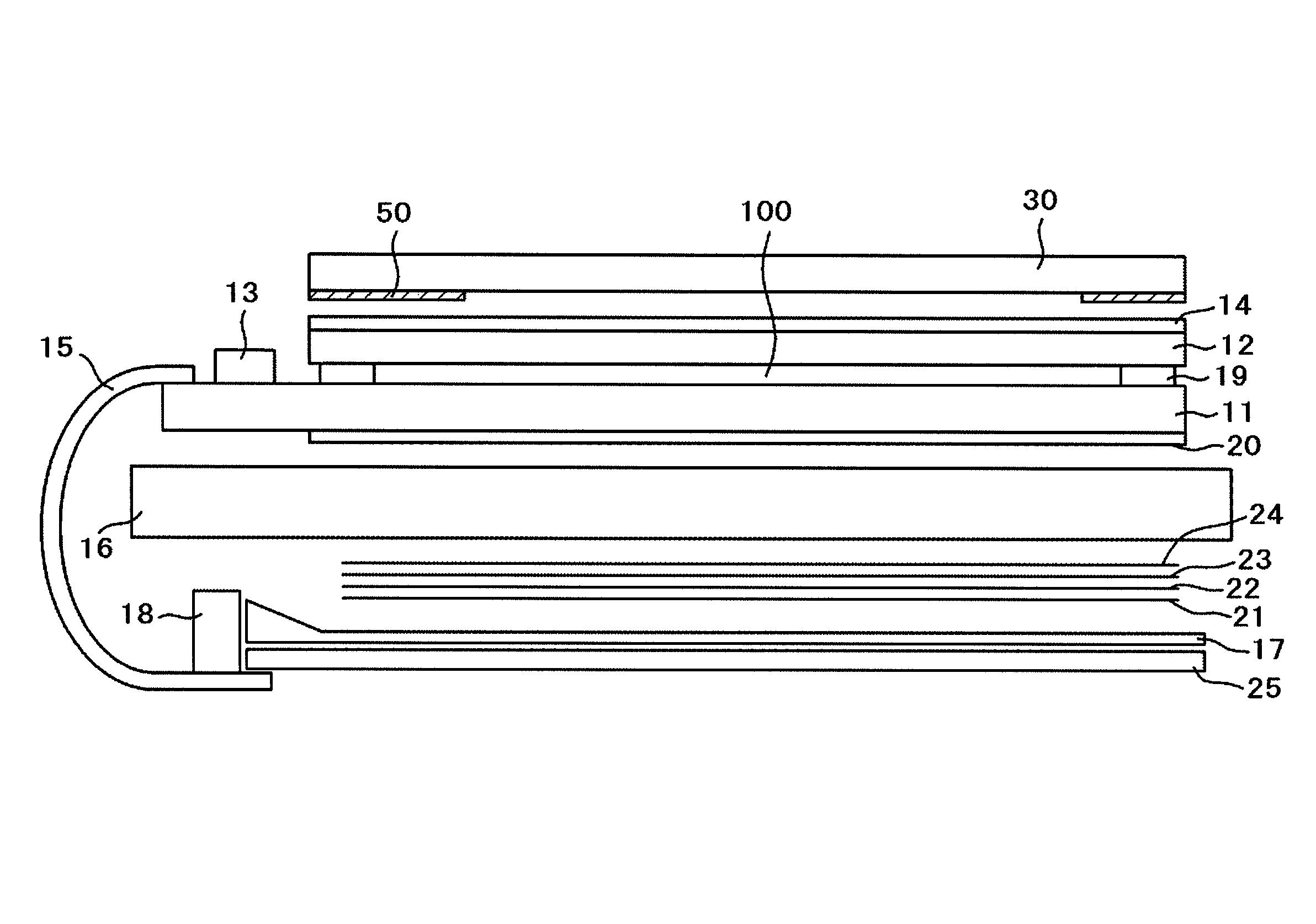
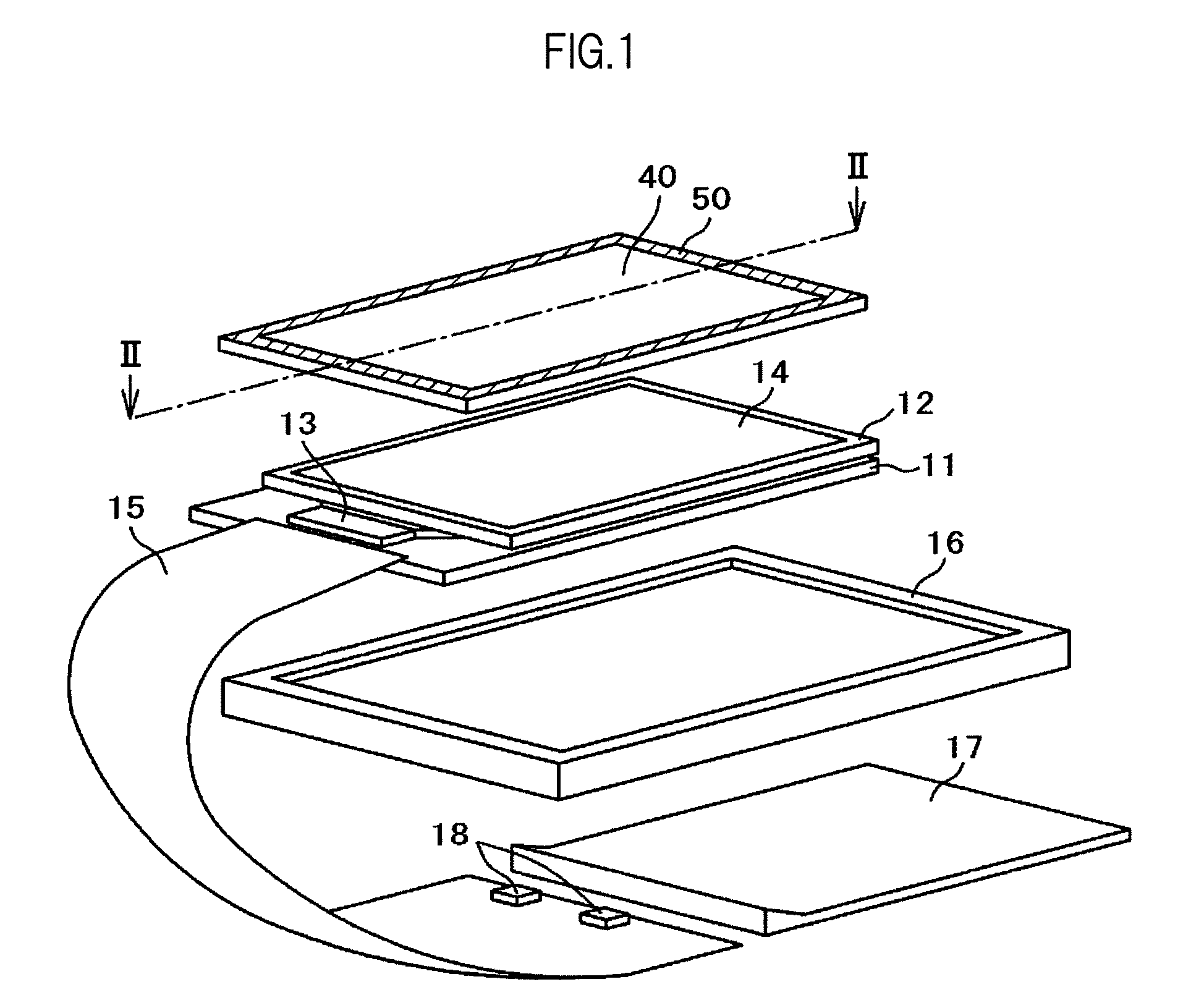
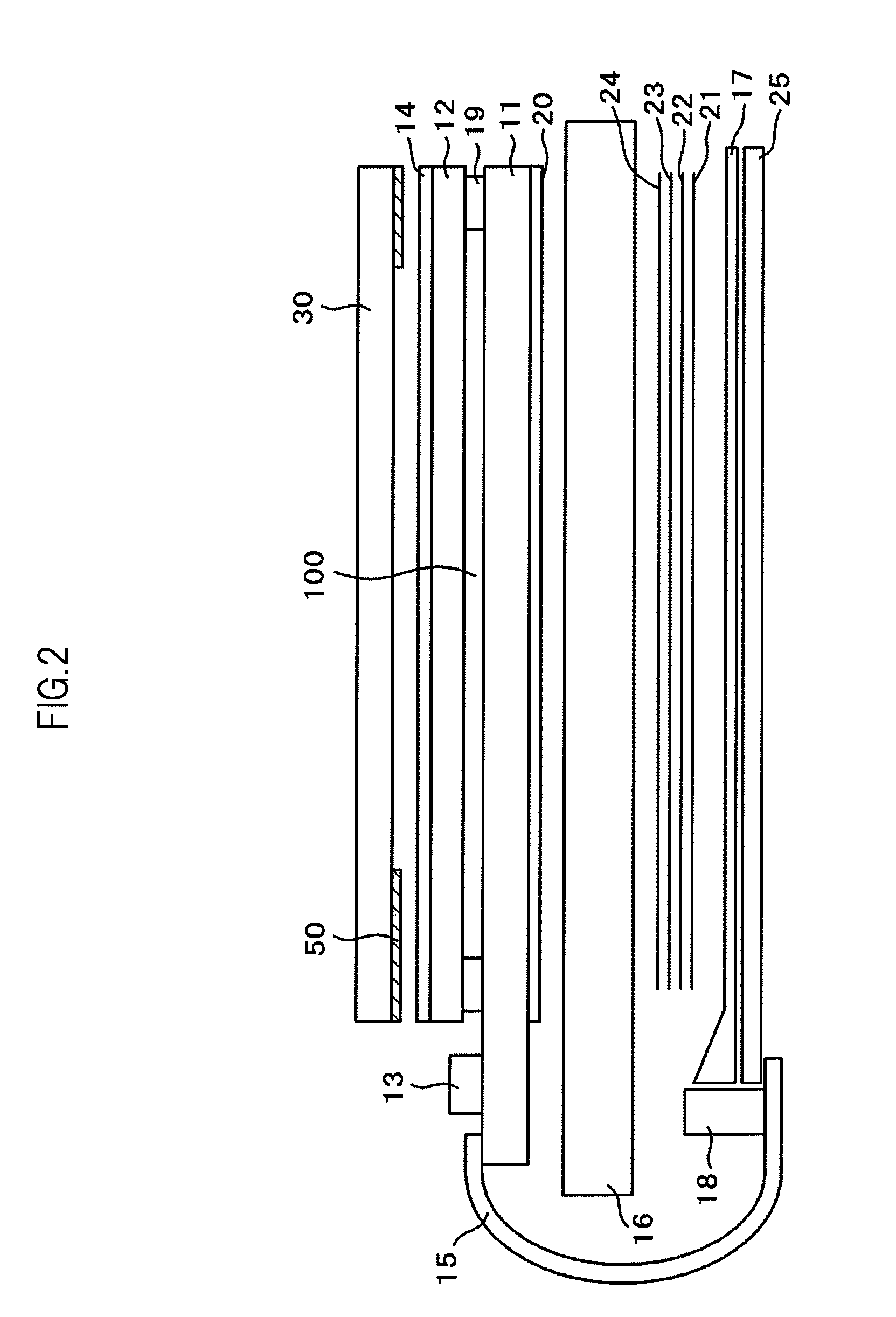
[0046]FIG. 1 is an exploded perspective view illustrating a liquid crystal display device according to a first embodiment of the present invention. FIG. 2 is a sectional view taken along the line II-II of FIG. 1. In FIG. 1, a liquid crystal display panel is constituted of a TFT substrate 11 and a color filter substrate 12. Pixel electrodes are formed on the TFT substrate 11 in matrix. Thin film transistors (TFTs) for changing over a signal supplied to respective pixel electrodes are also formed on the TFT substrate 11. The color filter substrate 12 which has color filters formed thereon is arranged to face the TFT substrate 11 in an opposed manner.

[0047]Respective thicknesses of glass substrates used in the manufacture of the TFT substrate 11 and the color filter substrate 12 are set to 0.5 mm. After completion of manufacturing of the liquid crystal display panel by charging and sealing liquid crystal between the substrates, outer sides of the liquid crystal display panel are polish...

second embodiment

[0078]Sometimes air bubbles are trapped when the face plate 30 is bonded to the liquid crystal display panel, or the bonding fails in other respects, resulting in defective products. In such cases, the face plate 30 is peeled off of the liquid crystal display panel in order to salvage the face plate 30 and the liquid crystal display panel. To separate the liquid crystal display panel and the face plate 30 from each other, a thin, thread-like material is inserted between one of the two surfaces of the pressure-sensitive adhesive material 35 and a surface that is in contact with this surface. For example, the thin, thread-like material is inserted in a part A of FIG. 7.

[0079]The face plate 30 and the liquid crystal display panel after separated from each other are illustrated in FIGS. 8A and 8B. FIG. 8A illustrates the face plate 30 with the pressure-sensitive adhesive material peeled off, and FIG. 8B illustrates the upper polarizer 14 of the liquid crystal display panel with the pres...

third embodiment

[0096]FIG. 13 is a sectional view illustrating a third embodiment of the present invention. In FIG. 13, the frame 50 is formed from four printed layers. The thermal expansion of the face plate 30 causes stress in a part where the frame 50 is formed. One of the factors for this is a sharp change in thickness of the adhesive material 31 or the pressure-sensitive adhesive material 35.

[0097]In this embodiment, the stress on the pressure-sensitive adhesive material 35 is eased through a gradual change in thickness of the pressure-sensitive adhesive material 35 which is accomplished by shifting the position of the edge of the frame 50 each time a new layer is printed. The frame 50 of FIG. 13 has four layers, and the edge of any one of the printed layers is receded toward the outside compared to one layer below this layer. Specifically, the second layer is receded by R1 from the first layer, the third layer is receded by R2 from the second layer, and the fourth layer is receded by R3 from ...


PUM

PropertyMeasurementUnit
thicknessaaaaaaaaaa
thicknessesaaaaaaaaaa
thicknessaaaaaaaaaa

Abstract

A face plate on which a frame is formed for improved design aesthetics is bonded to a top surface of an upper polarizer of a liquid crystal display panel with a pressure-sensitive adhesive material. The frame on the face plate is formed from five layers of printing. The pressure-sensitive adhesive material has a three-layer structure having a first pressure-sensitive adhesive member, a base material, and a second pressure-sensitive adhesive member. The first pressure-sensitive adhesive member is formed thicker than the second pressure-sensitive adhesive member, and hence the pressure-sensitive adhesive material can maintain a necessary thickness above the frame formed on the face plate. The reliability of adhesion between the face plate and the liquid crystal display panel is thus improved.

Description

CROSS-REFERENCE TO RELATED APPLICATION[0001]The present application claims priority from Japanese application JP 2008-071700 filed on Mar. 19, 2008, the content of which is hereby incorporated by reference into this application.BACKGROUND OF THE INVENTION[0002]1. Field of the Invention[0003]The present invention relates to a display device, and more particularly, to a technique of enhancing strength and visibility of a miniaturized liquid crystal display device used in a mobile phone or the like.[0004]2. Description of the Related Art[0005]With respect to a liquid crystal display device, there has been a strong demand for the reduction of a thickness of a liquid crystal display panel along with a demand for the reduction of a profile size of a set while maintaining a screen at a fixed size. To decrease the thickness of the liquid crystal display panel, after manufacturing the liquid crystal display panel, an outer side of the liquid crystal display panel is polished to decrease the ...

Claims


Application Information

Patent Timeline
Patent Type & Authority Patents(United States)
IPC IPC(8): G02F1/1333G02F1/1335B32B7/06
CPCG02F1/1335G02F2201/50Y10T428/1059Y10T428/2848G02F2202/28C09K2323/05G02F1/1333
Inventor KUBOTA, HIDENAOMIWA, HIROAKI
Owner PANASONIC INTELLECTUAL PROPERTY CORP OF AMERICA
Why Eureka
Try Eureka