The marking device of the transistor
A technology of transistors and printing marks, applied in semiconductor/solid-state device manufacturing, manufacturing tools, laser welding equipment, etc., can solve the problems of poor printing quality and lack of positioning process, and achieve the effect of avoiding crooked printing and ensuring the quality of printing marks.
- Summary
- Abstract
- Description
- Claims
- Application Information
AI Technical Summary
Problems solved by technology
Method used
Image
Examples
Embodiment Construction
[0018] The present invention will be described in further detail below by means of specific embodiments:
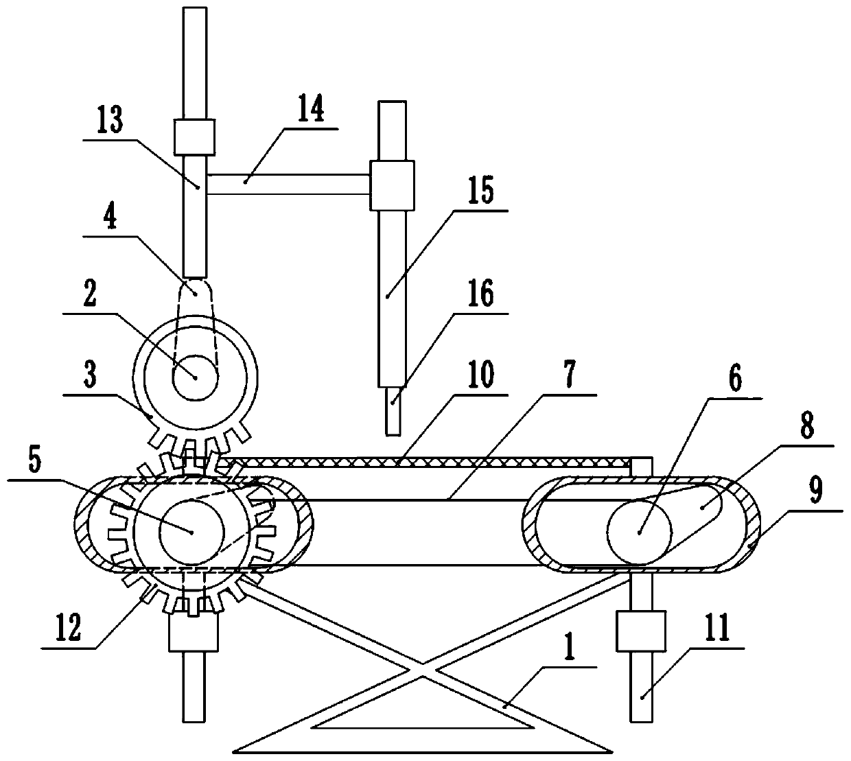
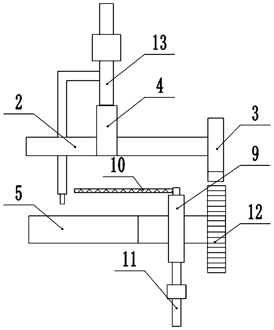
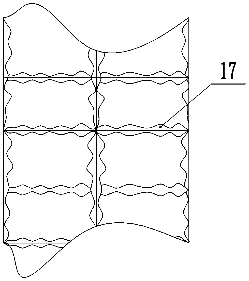
[0019] The reference signs in the accompanying drawings of the description include: frame 1, first drive shaft 2, notched gear 3, first cam 4, second drive shaft 5, third drive shaft 6, conveyor belt 7, second cam 8, abutment Ring 9, fixed net 10, slide bar 11, drive gear 12, push up bar 13, cross bar 14, mark bar 15, marking head 16, cleaning cotton 17.
[0020] Such as figure 1 , figure 2 , image 3 As shown: the marking device of the transistor, including a frame 1 and a driving mechanism, the driving mechanism includes a first driving shaft 2, the first driving shaft 2 is located above the frame 1, and one end of the first driving shaft 2 is connected to a motor. The other end of the first drive shaft 2 is coaxially fixedly connected with a notch gear 3, and the first drive shaft 2 is also fixedly connected with a first cam 4; a second drive shaft 5 and a third dr...
PUM
 Abstract
Description
Claims
Application Information


