
Method for direct ink-jet printing of short channel electrodes

An inkjet printing, short channel technology, applied in the direction of copying/marking method, printing, etc., can solve the problem of poor droplet ejection stability

Active Publication Date: 2018-06-15
SOUTH CHINA UNIV OF TECH
View PDF4 Cites 2 Cited by
  • Summary
  • Abstract
  • Description
  • Claims
  • Application Information

AI Technical Summary

Problems solved by technology

[0002] In order to reduce the channel length, researchers have made many attempts on the basis of improving the printing conditions such as substrate surface energy, temperature and nozzle piezoelectric waveform: (1) by reducing the nozzle (Sekitani T, Noguchi Y, Zschieschang U, et al. Organic transistors manufactured using inkjet technology with subfemtoliter accuracy[J].PROCEEDINGS OF THE NATIONAL ACAD EMY OF SCIENCES OFTHE UNITED STATES OF AMERICA.2008,105(13):4976-4980.) or obtained by using inkjet printing technologies such as EHD and SIJ 1-10μm channel length (Park J U, Hardy M, Kang S J, et al.High-resolution electrohydrodynamic j et printing.[J].Nature Materials.2007,6(10):782-789; Murata K, Matsumoto J, Tezuka A, et al. Super-fine ink-jet printing: towards the minimal manufacturing system[J]. ), this method is based on the premise of sacrificing the printing flux, and the droplet ejection stability is not as good as the traditional piezoelectric inkjet printing technology, which puts forward higher requirements for materials; (2) print a single electrode, and then ablate the channel by laser (Ko S H, Chung J, Choi Y H, et al. Laser based hybrid inkjet printing of nanoink for flexible electronics[M]. Proceedings of SPIE, Fieret J, Herman P R, Okada T, et al, 2005:5713, 97-104 .), the disadvantage is that it is usually not suitable for electronic devices with multilayer structures; (3) substrate photolithographic patterning forms dams that constrain droplet spreading (] Mahajan A, Hyun W J, Walker S B, et al.High-Resolution, Hi gh-Aspect RatioConductive Wires Embedded in Plastic Substrates[J].ACS Applied Materials&Interfaces.2015,7(3):1841-1847.), sacrificing the direct patterning advantage of inkjet printing technology; Pre-patterning (UV treatment (Suzuki K, Yutani K, Nakashima M, et al. Fabrication of All-printed Organic TFT Array on Flexible Substrate[J].2011,24(5):565-570.), photolithography or Plasma etching PI layer (Sirringhaus H, Kawase T, Friend R H, et a l.High-resolution inkjet printing of all-polymer transistor circuits.[J].MRS Bulletin.2001,290(7(Emerging Methods for Micro- and Nano-Fabrication Nanofabrication)):2123-2126.)), sacrificing the advantages of direct patterning of inkjet printing technology; (5) using the "coffee ring" effect to form adjacent thin lines (Bromberg V, Ma S, Singler T J .High-resolution inkj et printing of electrically conducting lines of silver nanoparticles by edge-enhanced twin-line deposition[J].Applied Physics Letters.2013,102(21):214101.), the disadvantage is that inkjet printing ink, substrate and the printing environment put forward certain requirements; (6) self-assembled monolayers using fluoride (deposition of CF 4 , plasma, or adding surfactants to reduce the surface energy of the first droplet) to treat the first droplet of ink so that it repels each other with the second droplet of ink to cause sliding, and self-aligns to form a 100nm-scale submicron channel (Noh Y Y, Zhao N, Caironi M, et al. Downscaling of self-aligned, all-printed polymer thin-film transistors [J]. Nature Nanotechnology. 2007, 2(12): 784-789; Sele C W, von Werne T, Friend R H, etal. Lithography-free, self-aligned inkjet printing with sub-hundred-nanometer resolution[J].AD VANCED MATERIALS.2005,17(8):997.); (7) Doggart et al. The hydrophobic boundary residue caused by the retraction of the first electrode was pre-printed on the substrate, and the second electrode was self-aligned to form short channels down to 10 μm (Doggart J, Wu Y, Liu P, et al. Facile Inkjet-Printing Self- Aligned Electrodes for Organic Thin-Film Transistor Arrays with Small and UniformChannel Length[J].ACS APPLIED MATERIALS&INTERFACES.2010,2(8):2189-2192.); (6), (7) Although the method is simple, it still needs Surface modification or request for hydrophilicity and hydrophobicity of the substrate and the material itself

Method used


Image

  • Method for direct ink-jet printing of short channel electrodes
  • Method for direct ink-jet printing of short channel electrodes
  • Method for direct ink-jet printing of short channel electrodes

Examples


Embodiment 1

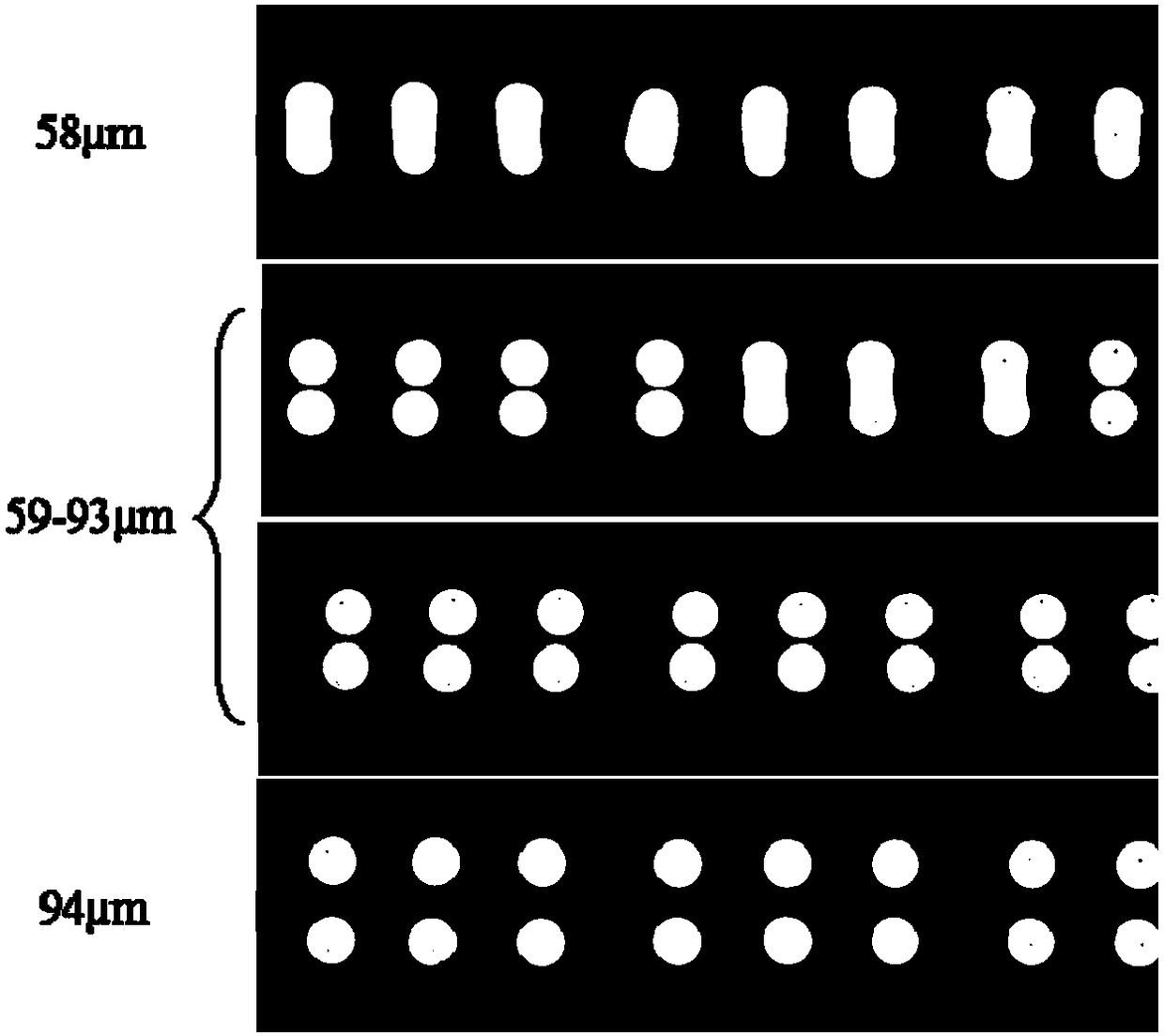
[0033] 1.1. Use granular silver ink (DGP-45LT-15C, Advanced Nano Products, South Korea) for droplet printing. Two droplets are used as a group to print droplet groups with different spacing. The distance between two adjacent droplets is at Between 58 and 94 μm (multiple groups of droplets with different spacing can be printed for easy observation), the printing parameters are: droplet spacing of 35 μm, ejection rate of 2m / s, substrate temperature of 30°C, and nozzle temperature of 30°C. The fusion rule of two printing droplets perpendicular to the printing direction changes with the increase of the droplet spacing as follows: figure 1 Shown: When the distance between droplets is 58μm (d 1 ) or less, the droplets are all fused; the droplet spacing is between 59 and 93 μm, and the droplets are separated, but at a small droplet spacing, the droplets merge sometimes; the droplet spacing is 94 μm (d 2 ) above, the droplets are all separated, and the distance between the droplets i...

Embodiment 2

[0041] 1, Figure 4 shown with 1.1 ( figure 1) with the same inkjet printing conditions (ink and printing parameters), and the marked value is the droplet distance. The obtained results prove that according to the steps described in Example 1 of the present invention, the short channel electrodes obtained parallel to and perpendicular to the printing direction can be repeated.

Embodiment 3

[0043] 1. Use granular silver ink (DGP-45LT-15C, Advanced Nano Products, South Korea) for short-channel electrode array printing. The printing parameters are: droplet spacing 35μm, jetting speed 2m / s, substrate temperature 30°C, nozzle temperature 30°C, d 1 = 58 μm, d 2 = 94 μm. at minimum d 1 、d 2 Starting from the set value of -1, gradually expand the range within a deviation of 10 μm, with a step size of 1 μm, to find the value that can print short channel arrays. Dm = 53 µm, Dn = 90 µm.

[0044] like Figure 5 As shown, all the channel lengths are less than 10 μm, and the channels are smooth. Figure 5 The SEM photo of B proves that there are no stray solute particles in the middle of the channel, and there is no possibility of short circuit between electrodes.


PUM


Abstract

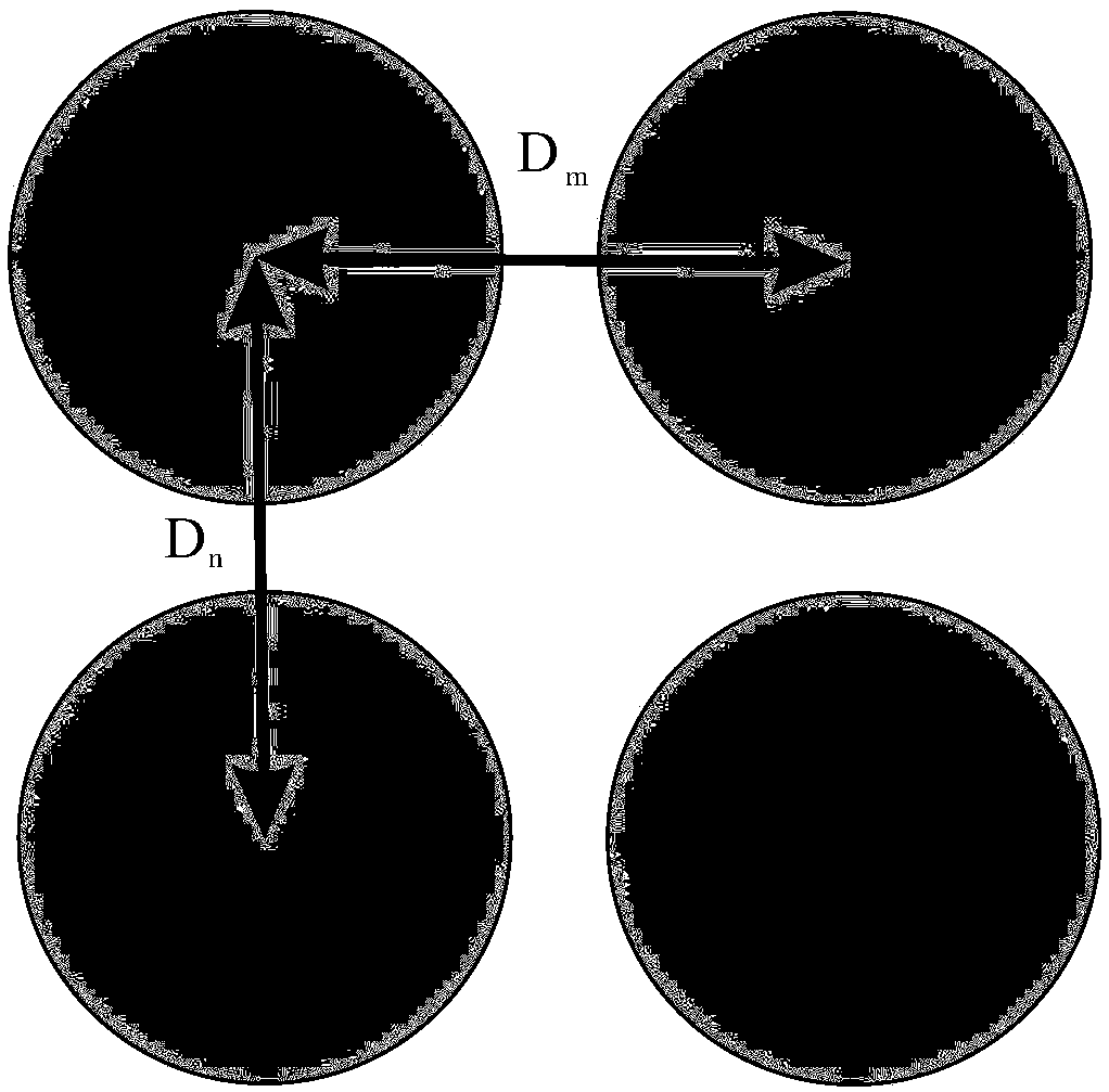
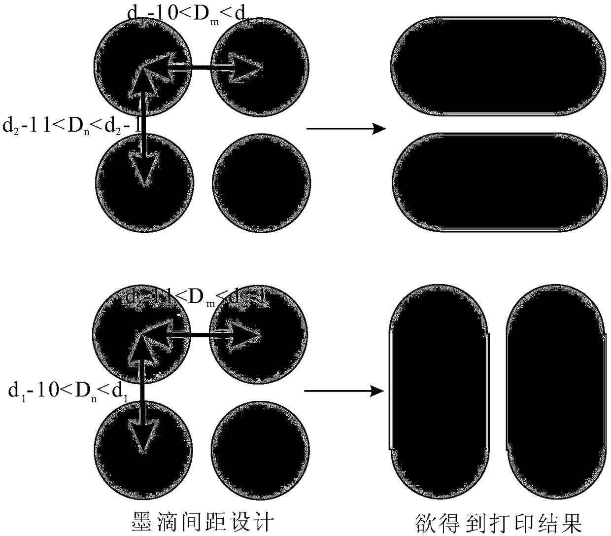
The invention discloses a method for direct ink-jet printing of short channel electrodes. The method comprises the following steps: (1) two-drop printing: ink-jet printing two-point fusion rules are explored to obtain a drop gap d1 of two drops from separation to total fusion and a drop gap d2 of the two drops from shorter distance to longer distance; and (2) four-drop printing: (1) a drop gap parallel to a printing direction is set as Dm, and a drop gap perpendicular to the printing direction is set as Dn, so that a range of drop gaps of the short channel electrodes parallel to the printing direction is Dm larger than d1-10 and not larger than d1 and Dn larger than d2-11 and smaller than d2, and a range of drop gaps of the short channel electrodes perpendicular to the printing direction is Dm larger than d2-11 and smaller than d2 and Dn larger than d1-10 and not larger than d1; and (2) multi-set printing experiment screening is performed in the obtained ranges to obtain the shot channel electrodes. The method is simple, can be repeated, and can be used for array printing.

Description

technical field [0001] The invention relates to the field of preparation of printed electronic devices, in particular to a method for direct inkjet printing of short channel electrodes. Background technique [0002] In order to reduce the channel length, researchers have made many attempts on the basis of improving the printing conditions such as substrate surface energy, temperature and nozzle piezoelectric waveform: (1) by reducing the nozzle (Sekitani T, Noguchi Y, Zschieschang U, et al. Organic transistors manufactured using inkjet technology with subfemtoliter accuracy[J].PROCEEDINGS OF THE NATIONAL ACAD EMY OF SCIENCES OFTHE UNITED STATES OF AMERICA.2008,105(13):4976-4980.) or obtained by using inkjet printing technologies such as EHD and SIJ 1-10μm channel length (Park J U, Hardy M, Kang S J, et al.High-resolution electrohydrodynamic j et printing.[J].Nature Materials.2007,6(10):782-789; Murata K, Matsumoto J, Tezuka A, et al. Super-fine ink-jet printing: towards the...

Claims


Application Information

Patent Timeline
Patent Type & Authority Applications(China)
IPC IPC(8): B41M5/00
CPCB41M5/0047
Inventor 宁洪龙陶瑞强姚日晖陈建秋杨财桂周艺聪蔡炜朱镇南魏靖林彭俊彪
Owner SOUTH CHINA UNIV OF TECH
Learn More