Power aging method and aging device for semiconductor power modules

A technology of power modules and semiconductors, which is applied in semiconductor/solid-state device manufacturing, electrical components, circuits, etc., and can solve problems such as high energy consumption in burn-in processing and complex system architecture

Pending Publication Date: 2018-07-06
SHENZHEN ZHENHUA MICROELECTRONICS
View PDF0 Cites 3 Cited by
  • Summary
  • Abstract
  • Description
  • Claims
  • Application Information

AI Technical Summary

Problems solved by technology

The signals driving each semiconductor power module for burn-in processing are independently generated and transmitted t

Method used


Image

  • Power aging method and aging device for semiconductor power modules

Examples


Embodiment Construction

[0020] The present invention will be described in further detail below in conjunction with the accompanying drawings and specific embodiments. It should be understood that the following exemplary embodiments and descriptions are only used to explain the present invention, not as a limitation to the present invention, and, in the case of no conflict, the embodiments in the present invention and the features in the embodiments can be combined with each other .

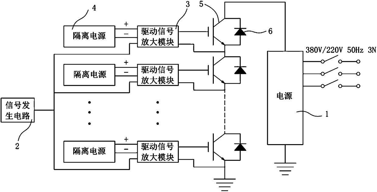
[0021] Such as figure 1 As shown, an embodiment of the present invention provides a power burn-in method for a semiconductor power module, which is mainly used for power burn-in of a semiconductor power module 5 composed of IGBT or MOS tubes. The burn-in method includes the following steps:

[0022] Connect multiple semiconductor power modules 5 to be aged in series, wherein the first pole of the first semiconductor power module 5 is connected to the output positive pole of the power supply 1, and the first poles of the...


PUM


Abstract

The embodiments of the present invention provide a power aging method and aging device for semiconductor power modules. The aging method includes the following steps that: a plurality of semiconductorpower modules are connected in series, wherein the first pole of the first semiconductor power module is connected with the output positive pole of a power source, the first poles of the other semiconductor power modules are connected with the second poles of the previous semiconductor power modules respectively, the second pole of the last semiconductor power module is connected with the outputnegative pole of the power source, and the third poles of the semiconductor power modules are connected with driving signal amplifying modules in a one-to-one correspondence manner, wherein the driving signal amplifying modules are connected with isolated power sources in a one-to-one correspondence manner, and each driving signal amplifying module is connected with the same signal generating circuit; driving signals generated by the signal generating circuit are amplified by the amplifying modules, and the amplified driving signals drive the semiconductor power modules to be turned on and turned off according to setting modes; and when the semiconductor power modules are turned on, the power source outputs constant current, and the constant current flows through the series semiconductor power modules, so that aging treatment can be performed on the series semiconductor power modules.

Description

technical field [0001] Embodiments of the present invention relate to the technical field of power burn-in of power modules, and in particular to a power burn-in method and burn-in device for semiconductor power modules. Background technique [0002] As a high-power semiconductor power switching device, the semiconductor power module composed of IGBT or MOS tube is widely used in frequency conversion and speed regulation of motors, various high-performance power supplies, industrial electrical automation and other fields, and has a broad market. Semiconductor power modules need aging treatment before leaving the factory. The aging treatment takes a long time, especially for the aging treatment of military semiconductor power modules. According to military specifications, each semiconductor power module must be subjected to at least 160 hours. For power aging screening, at least 1,000 hours of power aging are required for identification. [0003] In the existing burn-in proc...

Claims


Application Information

Patent Timeline
IPC IPC(8): H01L21/67
CPCH01L21/67271
Inventor 李迪伽谢永梁陈建功李加取元金皓
Owner SHENZHEN ZHENHUA MICROELECTRONICS
Why Eureka
Try Eureka