Versatile process for precision nanoscale manufacturing

A substrate and covering technology, applied in the general process field of precision nanoscale manufacturing, can solve the problems of constrained versatility, lack of film thickness range and resolution, etc.

Pending Publication Date: 2018-07-31
BOARD OF RGT THE UNIV OF TEXAS SYST
View PDF2 Cites 4 Cited by
  • Summary
  • Abstract
  • Description
  • Claims
  • Application Information

AI Technical Summary

Problems solved by technology

[0013] Therefore, currently used techniques for film deposition do not have the film thickness range and resolution required to be applicable to a wide range of fields, and have limited film thickness variations that can be achieved, thereby requiring changes in hardware to generate various profiles, thus constraining its generalizability across various applications

Method used


Image

  • Versatile process for precision nanoscale manufacturing
  • Versatile process for precision nanoscale manufacturing
  • Versatile process for precision nanoscale manufacturing

Examples


Embodiment Construction

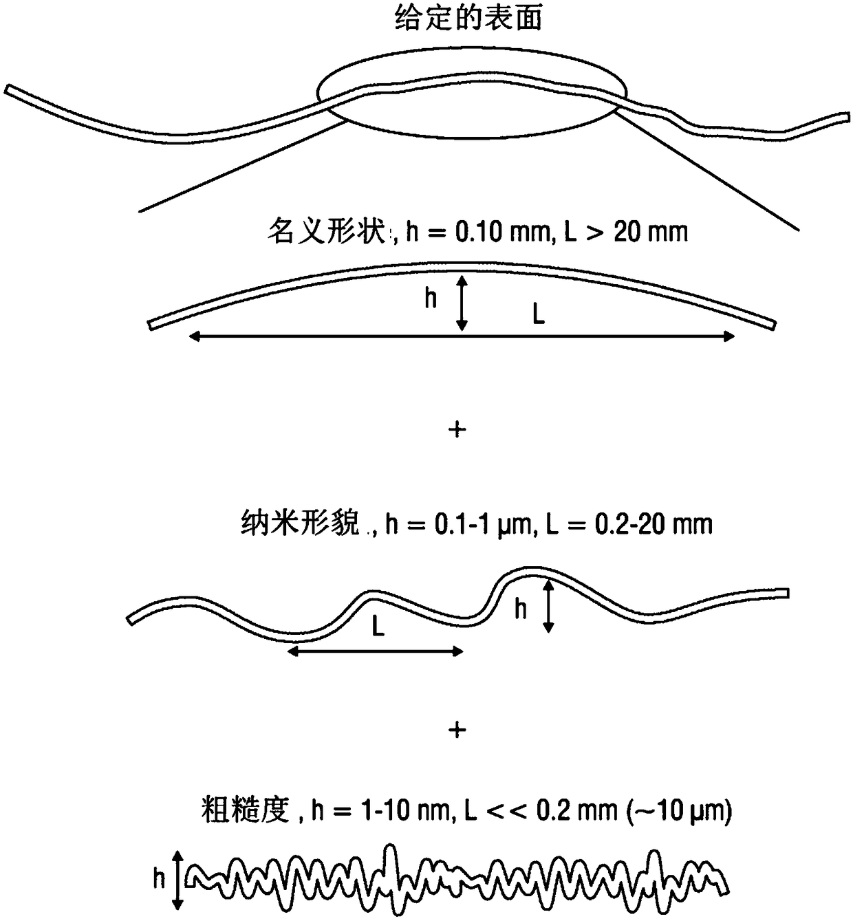
[0028] The present invention presents a general process for three types of precision nanoscale fabrication on both nominally planar substrates and substrates with nominally free-form shapes. As used herein, "nominal shape" refers to a desired shape, and it is assumed that standard manufacturing processes such as machining, diamond turning, and injection molding have achieved this nominal shape close to the ideal desired shape. This means that the nominal shape still has some parasitics beyond acceptable tolerances based on the intended use of the substrate.

[0029] These three types of nanoscale manufacturing (NM) include grinding (referred to herein simply as "NM1"), which involves changing the nominal shape of the substrate. For example, a planar substrate can be changed to a spherical nominal shape, or a spherical nominal shape can be changed to an aspheric surface, etc. The second type of nanoscale fabrication (NM) involves polishing (referred to herein simply as "NM2"),...


PUM

PropertyMeasurementUnit
thicknessaaaaaaaaaa

Abstract

A method for depositing thin films using a nominally curved substrate. Drops of a precursor liquid organic material are dispensed at a plurality of locations on a nominally curved substrate by one ormore inkjets. A superstrate is brought down on the dispensed drops to close the gap between the superstrate and the substrate thereby allowing the drops to form a contiguous film captured between thesubstrate and the superstrate. A non-equilibrium transient state of the superstrate, the contiguous film and the substrate is enabled to occur after a duration of time. The contiguous film is then cured to solidify it into a solid. The solid is separated from the superstrate thereby leaving a polymer film on the substrate. In this manner, such a technique for film deposition has the film thicknessrange, resolution and variation required to be applicable for a broad spectrum of applications.

Description

[0001] Cross References to Related Applications [0002] This application claims U.S. Provisional Patent Application Serial No. 62 / , entitled "Precision Systems and Processes for Programmable Deposition of Nanoscale Thin Films," filed October 15, 2015 242,147, which application is hereby incorporated by reference in its entirety. [0003] government interest [0004] This invention was made with government support under Grant No. ECCS1120823 awarded by the National Science Foundation. The US Government has certain rights in this invention. technical field [0005] The present invention relates generally to the fabrication of microdevices and nanodevices, and more particularly to a general process for precision nanoscale fabrication (e.g., trimming) on ​​both nominally planar substrates and substrates with nominally free-form shapes. , polishing and patterning). Background technique [0006] The fabrication of most micro- and nano-devices, including semiconductor, photoni...

Claims


Application Information

Patent Timeline
Patent Type & Authority Applications(China)
IPC IPC(8): B05D1/40B05D1/42B28B11/04B28B11/08
CPCB81C1/0038B05C5/027B05D1/42B05D3/067B05C5/0291B05C11/028B05C13/00B41J2/01
Inventor 希德加塔·V·斯林瓦森希拉旺·辛格哈尔
Owner BOARD OF RGT THE UNIV OF TEXAS SYST
Why Eureka
Try Eureka