Electronic device and control method thereof

An electronic device and controller technology, applied in hardware monitoring, electrical digital data processing, instruments, etc., can solve the problems of time-consuming, inability to measure the state of the chip with sensors, and inability to use, and achieve accurate chip performance analysis and continuous monitoring of chips. Status, effect of shortening time interval

Active Publication Date: 2018-08-10
REALTEK SEMICON CORP
View PDF5 Cites 0 Cited by
  • Summary
  • Abstract
  • Description
  • Claims
  • Application Information

AI Technical Summary

Problems solved by technology

However, when the user activates or reads the sensor through the user interface, most of the time is spent in the activation or reading process, so it is difficult to measure the continuous change of the chip state in a short time
In addition, in some specific applications, the user interface is disabled, so it is impossible to control the sensor to measure the chip status at this time through the user interface

Method used


Image

  • Electronic device and control method thereof
  • Electronic device and control method thereof
  • Electronic device and control method thereof

Examples


Embodiment Construction

[0015] The following disclosure provides many different embodiments or illustrations for implementing the features of the invention. The present disclosure may repeatedly refer to numerals and / or letters in different examples, and these repetitions are for simplification and illustration, and do not specify the relationship between different embodiments and / or configurations in the following discussion.

[0016] As used herein, "coupling" or "connection" can refer to two or more elements that are in direct physical or electrical contact with each other, or that are indirect physical or electrical contact with each other, and "coupling" or " "Connected" may also refer to the mutual operation or action of two or more elements.

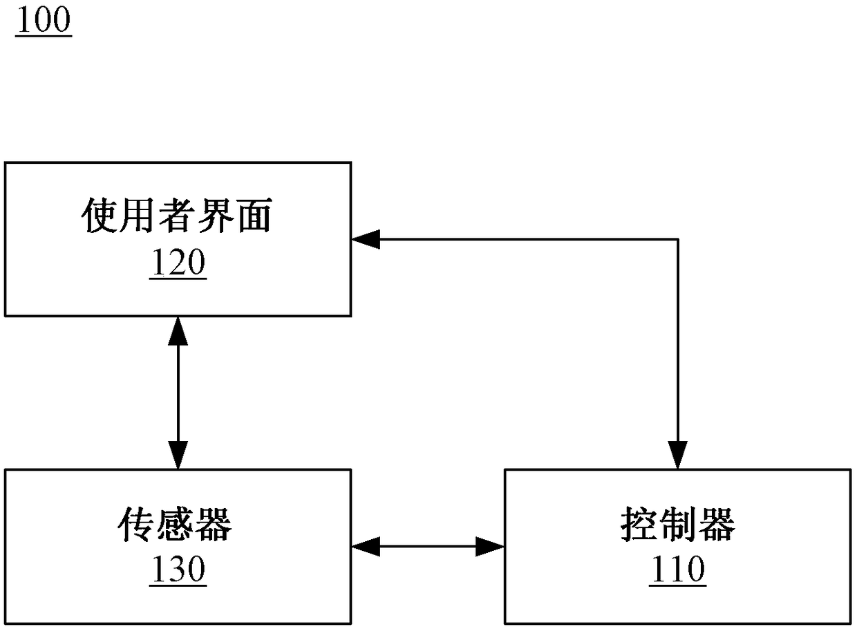
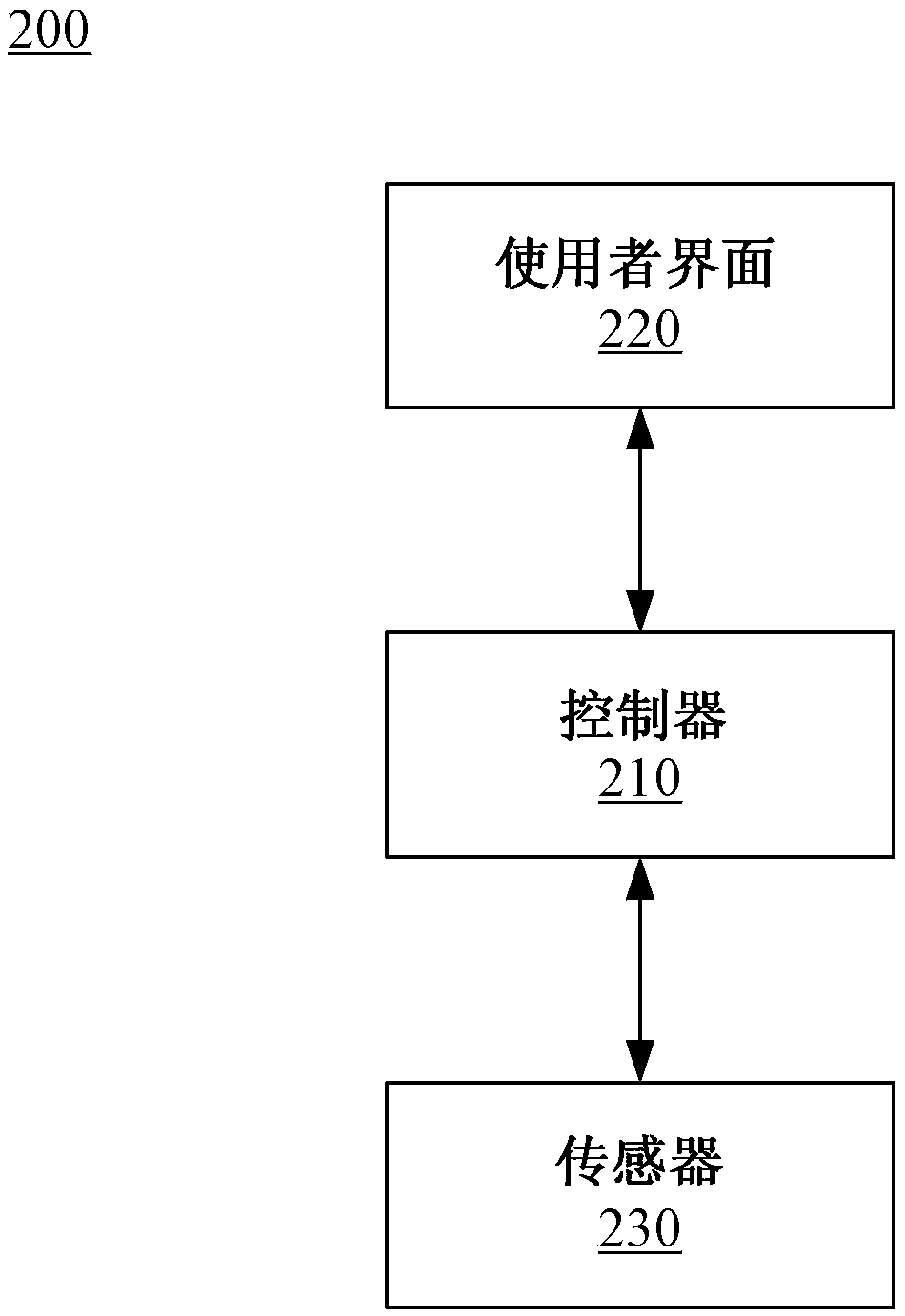
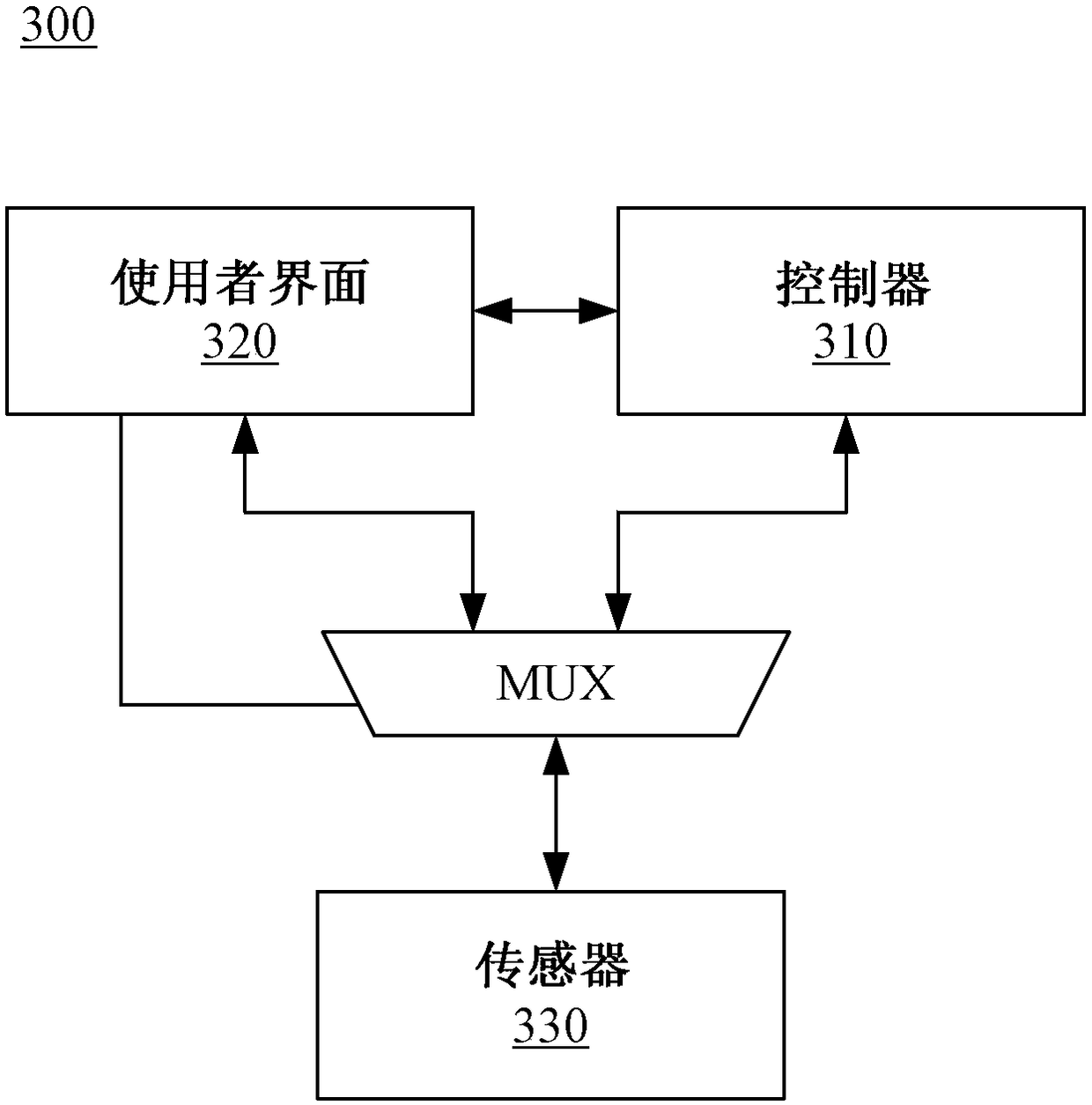
[0017] Please refer to figure 1 . figure 1 is a schematic diagram of an electronic device 100 according to an embodiment of the present invention. The electronic device 100 includes a controller 110 , a user interface 120 and a sensor 130 . The user ...


PUM


Abstract

The invention relates to an electronic device and a control method thereof. The electronic device includes a controller, a user interface and a sensor. The user interface and the sensor are coupled tothe controller. The user interface is used for sending a first user instruction to the controller in order to control the controller to enter an emergency mode. The controller is used for receiving the first user instruction to enter the emergency mode. The controller is controlled to continuously measure a chip or an environment of the chip to generate a plurality of sensing values, and sensingdata is generated according to the sensing values.

Description

technical field [0001] This application relates to an electronic device and its control method, and in particular to an electronic device and its control method for sensing chip state in burst mode. Background technique [0002] In the design of a system on chip (SOC), embedded sensors (such as voltage sensors, process variation sensors, speed sensors, and temperature sensors) are often used to monitor the state of the chip. However, when the user activates or reads the sensor through the user interface, most of the time is spent on the activation or reading process, so it is difficult to measure the continuous change of the chip state in a short time. In addition, in some specific applications, the user interface is not available, so the sensor cannot be controlled through the user interface to measure the state of the chip at this time. Contents of the invention [0003] One aspect of the present application is to provide an electronic device, which includes a controlle...

Claims


Application Information

Patent Timeline
IPC IPC(8): G06F11/30
CPCG06F11/3024G06F11/3055
Inventor 郭俊仪陈莹晏李日农
Owner REALTEK SEMICON CORP
Why Eureka
Try Eureka