Supercharge Your Innovation With Domain-Expert AI Agents!

Silicon wafer sorting machine

A technology for sorting machines and silicon wafers, which is applied in the fields of electrical components, semiconductor/solid-state device manufacturing, semiconductor/solid-state device testing/measurement, etc. It can solve the problems of low production efficiency and achieve the effect of improving production efficiency

Pending Publication Date: 2018-08-10
WUXI AUTOWELL TECH
View PDF0 Cites 10 Cited by
  • Summary
  • Abstract
  • Description
  • Claims
  • Application Information

AI Technical Summary

Problems solved by technology

[0004] In order to solve the problem that the silicon wafer sorting machine in the prior art can usually only complete a single inspection, resulting in low production efficiency, the embodiment of the present invention provides a silicon wafer sorting machine, which also includes a device for detecting external dimensions , hidden crack detection device, dirt detection device, thickness detection device, P / N type detection device at least two, of which:

Method used


Image

  • Silicon wafer sorting machine
  • Silicon wafer sorting machine
  • Silicon wafer sorting machine

Examples


Embodiment Construction

[0052] In order to make the object, technical solution and advantages of the present invention clearer, the implementation manner of the present invention will be further described in detail below in conjunction with the accompanying drawings.

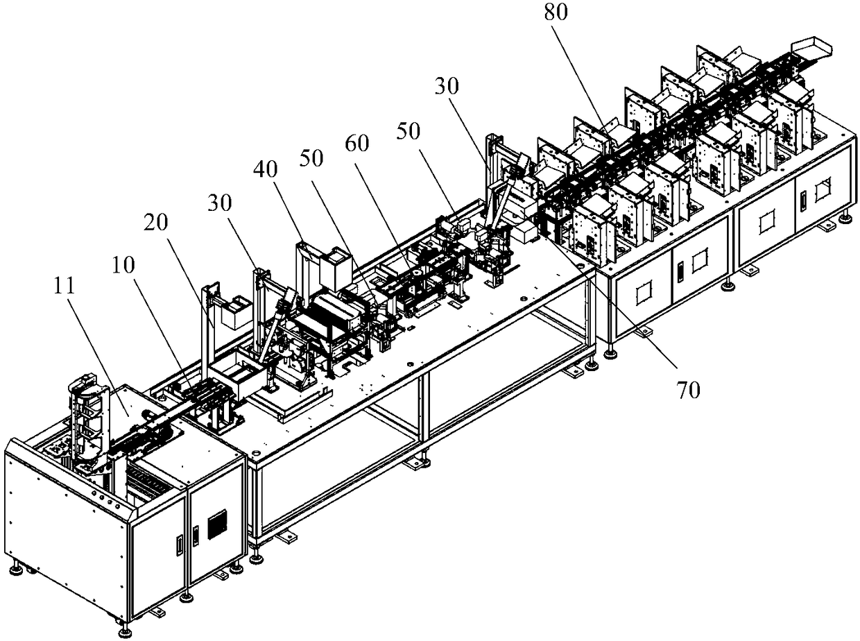
[0053] An embodiment of the present invention provides a silicon wafer sorting machine, the silicon wafer sorting machine includes a conveying line, and the silicon wafer sorting machine also includes a dimension detection device, a hidden crack detection device, a dirt detection device, and a thickness detection device , At least two of the P / N type detection devices, wherein:

[0054] Outline dimension detection device, used to detect whether the outline dimension of the silicon wafer conveyed on the conveying line is qualified;

[0055] The crack detection device is used to detect whether there are cracks on the silicon wafer;

[0056] A dirt detection device, used to detect whether there is dirt on the surface of the silicon wafer...


PUM


Abstract

The invention discloses a silicon wafer sorting machine, and belongs to the technical field of solar cell sheets. The silicon wafer sorting machine comprises at least two devices selected from an appearance size detection device, a hidden crack detection device, a dirty stain detection device, a thickness detection device and a P / N type detection device. The appearance size detection device is used for detecting whether the appearance size of a silicon wafer conveyed on a conveyor line is qualified or not. The hidden crack detection device is used for detecting whether a hidden crack exist onthe silicon wafer or not. The dirty stain detection device is used for detecting whether dirty stains exist on the surface of the silicon wafer or not. The thickness detection device is used for detecting whether the thickness of the silicon wafer is qualified or not. The P / N type detection device is used for detecting whether the silicon wafer is P-type or N-type. According to the silicon wafer sorting machine, the problems that in the prior art, a silicon wafer sorting machine can only complete the detection of a single item and the production efficiency is low, can be solved. Therefore, theeffect of improving the production efficiency of solar cell panels is achieved.

Description

technical field [0001] The invention relates to the technical field of solar cells, in particular to a silicon wafer sorting machine. Background technique [0002] In the production process of solar cells, silicon rods need to be cut into silicon wafers first, and then the silicon wafers need to be cleaned. After cleaning, multiple inspections are required on the silicon wafers, such as surface dirt, thickness, size and hidden cracks. detection. [0003] Traditional silicon wafer sorting machines usually can only complete a single inspection, and there is no automatic continuous operation between the transportation and inspection links, resulting in low production efficiency. Contents of the invention [0004] In order to solve the problem that the silicon wafer sorting machine in the prior art can only complete single-item detection, resulting in low production efficiency, the embodiment of the present invention provides a silicon wafer sorting machine, which also includ...

Claims


Application Information

Patent Timeline
IPC IPC(8): H01L21/66H01L21/67
CPCH01L21/67271H01L22/20Y02P70/50
Inventor 李文韦孟锑王美丁治祥徐康宁李昶黄浩桑俞
Owner WUXI AUTOWELL TECH
Features
  • R&D
  • Intellectual Property
  • Life Sciences
  • Materials
  • Tech Scout
  • Unparalleled Data Quality
  • Higher Quality Content
  • 60% Fewer Hallucinations
Learn More