A Fabrication Method of Metal Nanostructure Arrays Based on Interface Induced Growth

A metal nanostructure and metal induced technology, which is applied in the fields of nanotechnology, nanotechnology, and nanotechnology for materials and surface science to achieve the effect of simple process, easy large-area preparation, and good controllability

Active Publication Date: 2020-07-03
ANHUI NORMAL UNIV
View PDF7 Cites 0 Cited by
  • Summary
  • Abstract
  • Description
  • Claims
  • Application Information

AI Technical Summary

Problems solved by technology

However, due to the inevitable defects of colloidal 2D crystals, this method still has problems in large-area uniformity.

Method used


Image

  • A Fabrication Method of Metal Nanostructure Arrays Based on Interface Induced Growth
  • A Fabrication Method of Metal Nanostructure Arrays Based on Interface Induced Growth
  • A Fabrication Method of Metal Nanostructure Arrays Based on Interface Induced Growth

Examples


Embodiment 1

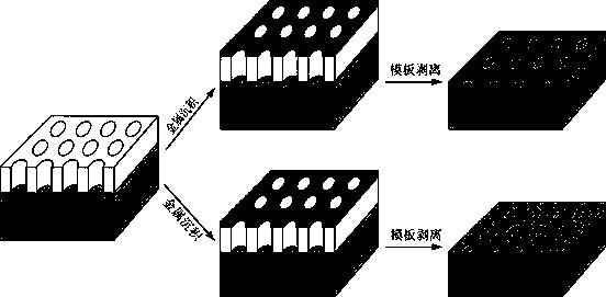
[0022] (1) Soak the silicon wafer in a mixed solution of concentrated sulfuric acid and hydrogen peroxide at 90°C for 1 hour, then ultrasonically clean it in propanol, ethanol, and deionized water for more than 15 minutes, then rinse it with a large amount of deionized water, and finally Blow dry with nitrogen.

[0023] (2) Drop a drop of water on the cleaned silicon wafer surface, and adhere the ultra-thin porous alumina template supported by polymethyl methacrylate (PMMA) to the silicon surface. Then the sample was soaked in propanol solution for 5-10 minutes, the PMMA layer was removed, the template was transferred to the silicon substrate, washed once with clean propanol solution, and dried in the air.

[0024] (3) The adhesion between the porous alumina template and the substrate is weak, and the sample is left to stand for several hours to further relax the adhesion between the template and the substrate.

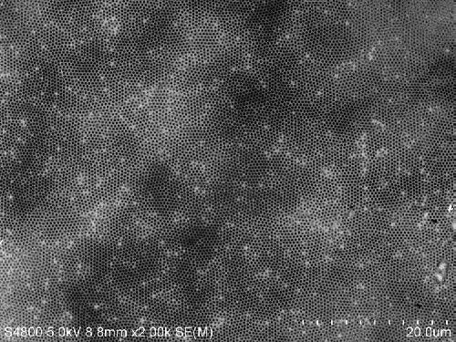
[0025] (4) The substrate with the alumina template on the surfa...

Embodiment 2

[0028] (1) Soak the silicon wafer in a mixed solution of concentrated sulfuric acid and hydrogen peroxide at 90°C for 1 hour, then ultrasonically clean it in propanol, ethanol, and deionized water for more than 15 minutes, then rinse it with a large amount of deionized water, and finally Blow dry with nitrogen.

[0029] (2) Drop a drop of water on the surface of the cleaned silicon wafer, and adhere the ultra-thin porous alumina template supported by PMMA to the surface of the silicon surface. Then the sample was soaked in propanol solution for 5-10 minutes, the PMMA layer was removed, the template was transferred to the silicon substrate, washed once with clean propanol solution, and dried in the air.

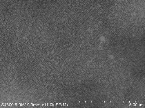
[0030] (3) The adhesion between the porous alumina template and the substrate is weak, and the adhesion between the template and the silicon substrate is strengthened by low-temperature annealing. The low-temperature annealing is carried out by a heating plate. 4 hours.

[0...

Embodiment 3

[0034] (1) Soak the silicon wafer in a mixed solution of concentrated sulfuric acid and hydrogen peroxide at 90°C for 1 hour, then ultrasonically clean it in propanol, ethanol, and deionized water for more than 15 minutes, then rinse it with a large amount of deionized water, and finally Blow dry with nitrogen.

[0035] (2) Drop a drop of water on the surface of the cleaned silicon wafer, and adhere the ultra-thin porous alumina template supported by PMMA to the surface of the silicon surface. Then the sample was soaked in propanol solution for 5-10 minutes, the PMMA layer was removed, the template was transferred to the silicon substrate, washed once with clean propanol solution, and dried in the air.

[0036] (3) The adhesion between the porous alumina template and the substrate is weak, and the sample is left to stand for several hours to further relax the adhesion between the template and the substrate.

[0037] (4) The substrate with the alumina template on the surface w...


PUM

PropertyMeasurementUnit
thicknessaaaaaaaaaa

Abstract

The invention relates to the manufacturing method of a metal nanostructure array based on interface induction growth. The method comprises the following steps of 1, cleaning a substrate; 2, transferring a template, and transferring an ultrathin porous alumina template to the cleaned substrate; adjusting an adhesive force, standing a sample acquired from the step2 for several hours so that an adhesive force portion between the template and the substrate is relaxed, or through low temperature annealing, strengthening the adhesive force between the template and the substrate; 4, depositing metal,and depositing the metal on the surface of the sample obtained from the step3 by using a physical vapor deposition method; and 5, peeling the template, after the deposition is completed, using an adhesive tape to peel the template so that an ordered metal nanostructure array is left on the surface of the substrate, wherein under an adhesive force relaxation condition, an ordered nano-pore array is acquired, and under an adhesive force strengthening condition, an ordered nano-ring array is acquired. The technology of the method is simple, cost is low, and the method can be expanded to a waferscale.

Description

technical field [0001] The invention relates to a method for preparing a metal nanostructure array, in particular to a method for preparing a metal nanostructure array based on interface-induced growth, and belongs to the technical field of nanomaterial preparation. Background technique [0002] Surface plasmons are the collective oscillations of conduction electrons on the metal surface under the excitation of the incident photoelectric magnetic field, which makes the metal nanostructures exhibit some peculiar optical properties, which has attracted widespread attention. It has great application prospects in many fields. By controlling the shape, size, dielectric environment of the metal nanostructure, and the type, period, and spacing of the array, its surface plasmon optical properties can be effectively regulated to meet specific application requirements. Metal nanostructures with various shapes can be prepared by using micro-nano processing technologies, such as electr...

Claims


Application Information

Patent Timeline
Patent Type & Authority Patents(China)
IPC IPC(8): H01L21/02B82Y30/00B82Y40/00
CPCB82Y30/00B82Y40/00H01L21/02521H01L21/0259H01L21/02612
Inventor 左则文闻壹兵
Owner ANHUI NORMAL UNIV
Why Eureka
Try Eureka