Silicon chip classification method by means of laser code printing discrimination

A technology of laser coding and laser coding, which is applied in the field of single crystal silicon wafer classification, can solve the problems of unqualified silicon wafers, difficulty in identifying photoelectric parameters, etc., and achieve the effect of avoiding wrong selection

Inactive Publication Date: 2018-08-17
XINGTAI JINGLONG ELECTRONICS MATERIAL
View PDF5 Cites 5 Cited by
  • Summary
  • Abstract
  • Description
  • Claims
  • Application Information

AI Technical Summary

Problems solved by technology

[0003] The purpose of the present invention is to provide a method for laser coding to distinguish silicon wafer classification, so as to solve the technical problem in the prior art that it is difficult to identify silicon wafers with unqualified photoelectric parameters after slicing silicon rods

Method used


Image

  • Silicon chip classification method by means of laser code printing discrimination

Examples


Embodiment Construction

[0019] In order to make the technical problems, technical solutions and beneficial effects to be solved by the present invention clearer, the present invention will be further described in detail below in conjunction with the accompanying drawings and embodiments. It should be understood that the specific embodiments described here are only used to explain the present invention, not to limit the present invention.

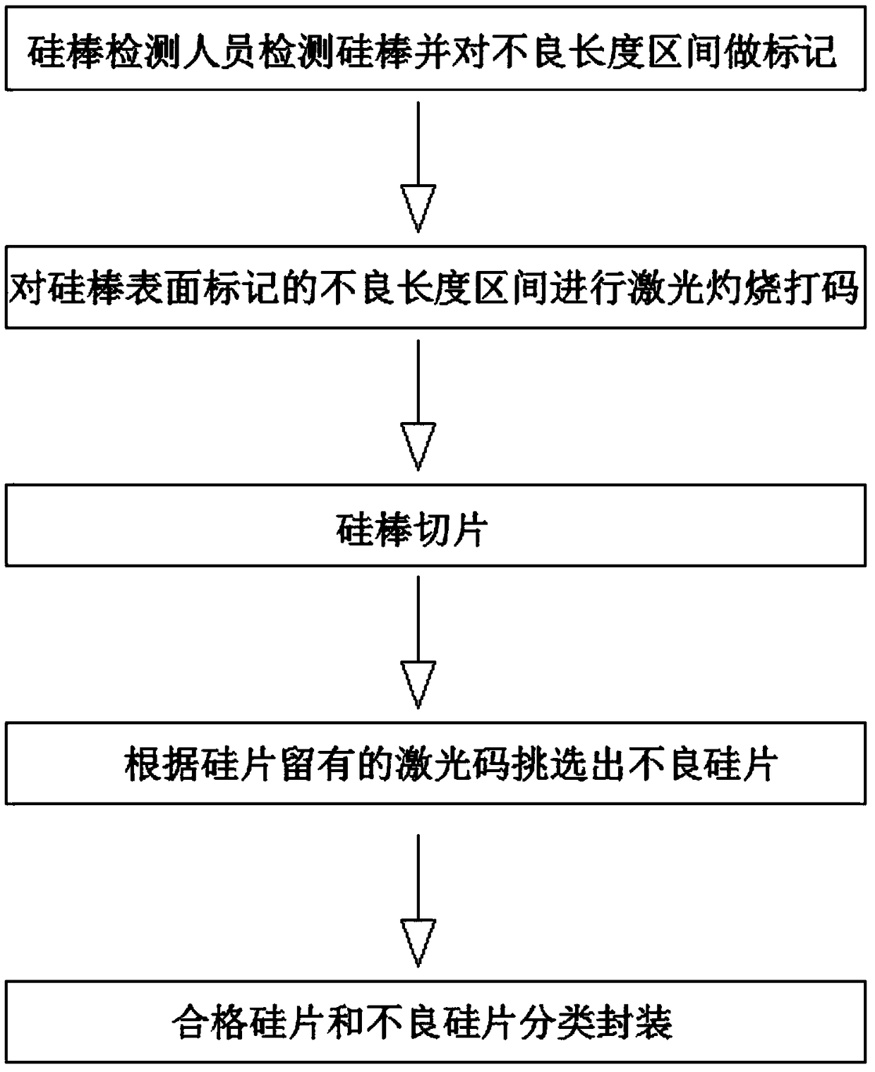
[0020] A method for classifying silicon wafers by laser marking provided by the present invention will now be described. A method for laser coding to determine the classification of silicon wafers, comprising the following steps:

[0021] (1) Silicon rod inspectors detect the surface of the silicon rod and mark the bad length interval: after the monocrystalline silicon rod is formed, different positions in the length direction have different photoelectric parameters, and the photoelectric parameters of some position intervals cannot reach the production of solar pa...


PUM

PropertyMeasurementUnit
widthaaaaaaaaaa
thicknessaaaaaaaaaa
thicknessaaaaaaaaaa

Abstract

The invention provides a silicon chip classification method by means of laser code printing discrimination, and belongs to the technical field of classification of monocrystalline silicon chips. The silicon chip classification method by means of laser code printing discrimination includes the following steps: 1) a silicon rod inspector detects a silicon rod and makes marks for adverse length intervals; 2) laser burning code printing is performed on the adverse length intervals marked on the surface of the silicon rod; 3) the silicon rod is sliced; 4) according to the laser codes on silicon chips, adverse silicon chips are selected; and 5) qualified silicon chips and adverse silicon chips are packaged after classification. The silicon chip classification method by means of laser code printing discrimination makes permanent laser codes on the surface of the unqualified intervals of the photoelectric parameters of the silicon rod through laser burning and code printing, and after the silicon rod is sliced into silicon chips, the laser codes are maintained on the silicon chips with unqualified photoelectric parameters and do not disappear because of washing and polishing of the siliconchips, thus avoiding the selection error caused in the flowing process.

Description

technical field [0001] The invention belongs to the technical field of monocrystalline silicon wafer classification, and more specifically relates to a method for identifying silicon wafer classification by laser coding. Background technique [0002] The photoelectric parameters of the single crystal silicon rod need to be tested before slicing, and the detected photoelectric parameters are not qualified. The existing classification method is to record the unqualified interval length of photoelectric parameters, convert the number of unqualified silicon wafers according to the interval length and the thickness of the cut silicon wafers, and record the converted number of unqualified silicon wafers On the follow-up work order, the unqualified silicon wafers are picked out after the silicon wafer processing process, because there are many transfer links from silicon rods to silicon wafers, it is easy to lose the receipt or the order of the silicon wafers is confused during the...

Claims


Application Information

Patent Timeline
Patent Type & Authority Applications(China)
IPC IPC(8): H01L21/02H01L21/66B28D1/22
CPCB28D1/22H01L21/0201H01L22/26
Inventor 王会敏张浩强李立伟吕思迦孙毅
Owner XINGTAI JINGLONG ELECTRONICS MATERIAL
Why Eureka
Try Eureka