A binding mark identification device and binding equipment

A technology for identifying devices and markings, applied in instruments, nonlinear optics, optics, etc., can solve problems that affect the appearance of displays, and achieve the effect of avoiding high process requirements

Active Publication Date: 2020-11-17
BOE TECH GRP CO LTD +1
View PDF5 Cites 0 Cited by
  • Summary
  • Abstract
  • Description
  • Claims
  • Application Information

AI Technical Summary

Problems solved by technology

like figure 2 As shown, the other is to not coat the black ink material in the binding mark 3 area, and coat the black ink material in the other peripheral routing areas. This solution affects the appearance of the display due to the design of the opening 10 in the binding mark area

Method used


Image

  • A binding mark identification device and binding equipment
  • A binding mark identification device and binding equipment
  • A binding mark identification device and binding equipment

Examples


Embodiment 1

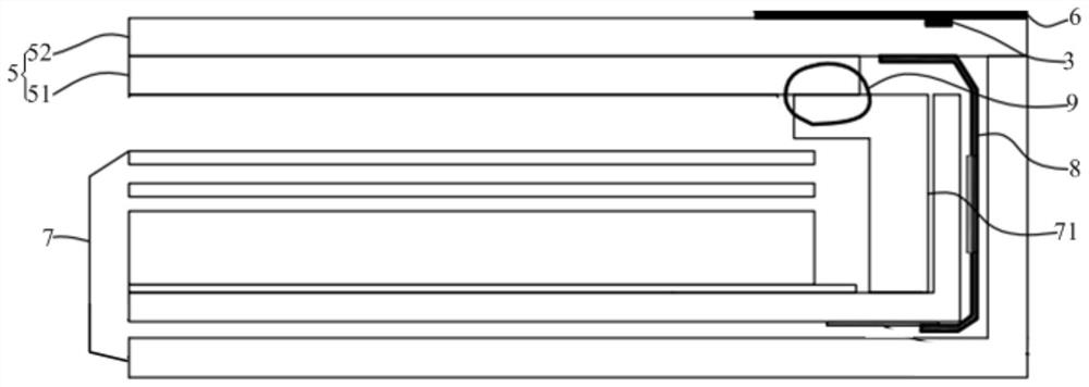
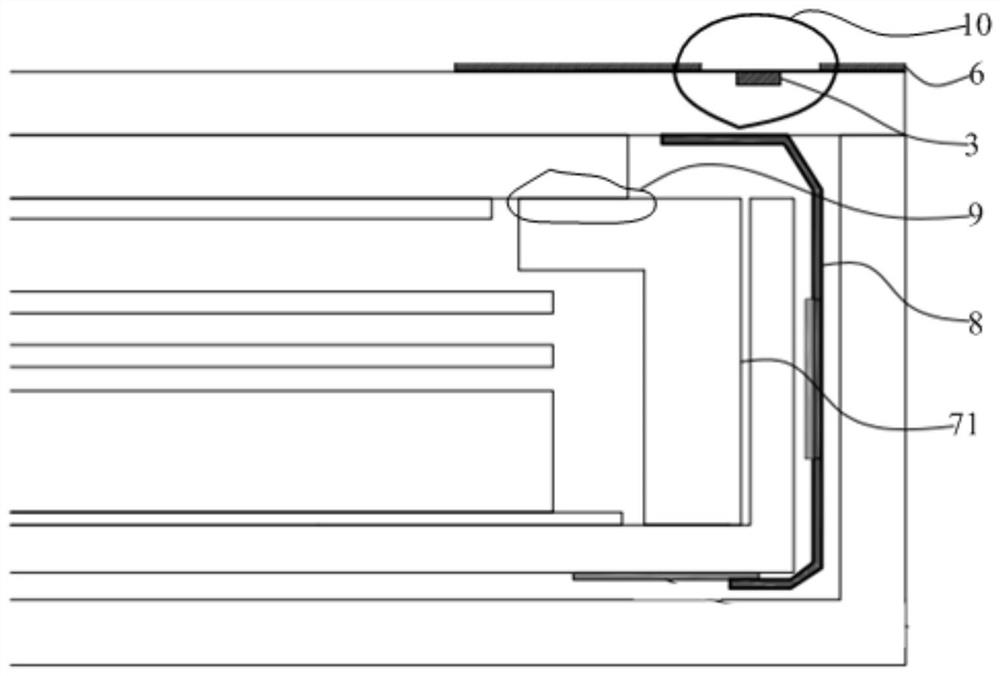
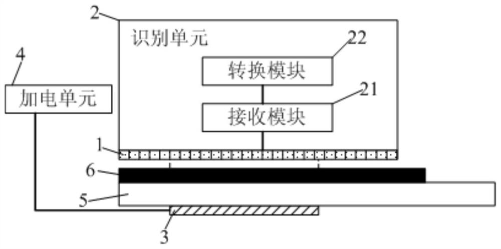
[0036] This embodiment provides a binding mark identification device, such as image 3 As shown, the identification device includes an induction unit 1 and an identification unit 2. The setting position of the induction unit 1 corresponds to the binding mark 3, and the induction unit 1 can induce a charge when the binding mark 3 is powered on; the identification unit 2 is connected to the induction unit 1, It is used for receiving the induced charge of the sensing unit 1, and identifying the binding marker 3 according to the induced charge.

[0037] Wherein, the binding mark 3 is formed by conductive material. By setting the induction unit 1 and the identification unit 2, when the binding mark 3 is powered on, the charge can be induced on the induction unit 1, and the identification unit 2 can identify the binding mark 3 according to the induced charge, so that the binding mark 3 can be realized. 3 can be normally identified even when it is covered by black ink, thereby avoid...

Embodiment 2

[0051] This embodiment provides a binding mark identification device, which is different from Embodiment 1, such as Figure 8 As shown, a part of the conductive sheet 12 is located on one side of the insulating base 11 , and another part of the conductive sheet 12 is located on the other side of the insulating base 11 .

[0052] Other structures of the binding mark recognition device in this embodiment are the same as those in Embodiment 1, and will not be repeated here.

[0053] Beneficial effects of embodiment 1-2: the binding mark recognition device provided in embodiment 1-2, by setting the sensing unit and the recognition unit, when the binding mark is powered on, the charge can be induced on the sensing unit, and the recognition unit The binding mark can be identified according to the induced charge, so that it can be recognized normally even when the binding mark is covered by black ink, thereby avoiding the opening design of the binding mark in the prior art (that is, ...

Embodiment 3

[0055] This embodiment provides a binding device, including the binding mark identification device in Embodiment 1 or 2.

[0056] By adopting the binding mark identification device in Embodiment 1 or 2, the binding device can be normally identified even when the binding mark is covered by black ink, so that the binding device can bind Normal in-position bonding of flexible printed circuit boards is also possible with markings covered in black ink.


PUM


Abstract

The invention provides a binding mark identification device and binding equipment. The binding mark recognition device includes a sensing unit and a recognition unit, the setting position of the sensing unit corresponds to the binding mark, and the sensing unit can induce electric charge when the binding mark is powered on; the recognition unit is connected to the sensing unit for receiving the induction of the sensing unit charge, and the bound label is recognized based on the induced charge. In the binding mark identification device, when the binding mark is powered on, the induction unit can induce electric charge, and the identification unit can identify the binding mark according to the induced charge, so that the binding mark can be recognized even when the binding mark is covered by black ink. It can be recognized normally, thereby avoiding the display appearance problem caused by the opening design of the binding mark in the prior art, and at the same time avoiding the use of black ink materials that can transmit light within a certain wavelength range in the prior art, thus avoiding the use of The problem of high process requirements brought by this black ink material.

Description

technical field [0001] The present invention relates to the field of display technology, in particular to a binding mark recognition device and binding equipment. Background technique [0002] In general, the four sides of the liquid crystal panel of the liquid crystal display are wrapped by an outer frame, and the outer frame is usually assembled with the rear shell of the display. The array substrate (TFT substrate) of the liquid crystal panel is arranged close to the backlight source, and the color filter substrate (CF substrate) is located on the side of the array substrate away from the backlight source. In contrast, as figure 1 As shown, the four-sided borderless liquid crystal display does not include the above-mentioned outer frame, and the liquid crystal panel is adhered to the middle frame 71 of the backlight 7 through the double-sided adhesive 9, so as to realize the borderless structure of the liquid crystal display. The color filter substrate 51 (CF substrate)...

Claims


Application Information

Patent Timeline
Patent Type & Authority Patents(China)
IPC IPC(8): G02F1/13
CPCG02F1/1303G02F1/13452G02F1/133512G02F1/133562G02F1/133308G02F1/133345G02F1/133354
Inventor 陈曦李东熙袁剑峰刘耀
Owner BOE TECH GRP CO LTD
Why Eureka
Try Eureka