Array substrate, manufacturing method thereof, and display device

An array substrate and display area technology, which is applied in semiconductor/solid-state device manufacturing, instruments, semiconductor devices, etc., can solve the problems of high resistance of transparent touch electrodes, inability to arrange metal leads densely, and low signal strength of touch signals. To achieve the effect of expanding the position range, reducing bad touch, and improving touch performance

Active Publication Date: 2021-03-26
BOE TECH GRP CO LTD +1
View PDF10 Cites 0 Cited by
  • Summary
  • Abstract
  • Description
  • Claims
  • Application Information

AI Technical Summary

Problems solved by technology

[0002] In touch products such as touch and display driver integration (Touch and Display driver Integration, TDDI), it is easy to generate touch due to the excessive resistance of the transparent touch electrode and the low signal strength of the received touch signal. poor control
For example, touch electrodes covering a display area of ​​5×5 mm generally need to export the collected touch signals to external chips through metal leads, because the number of metal leads cannot be densely arranged due to the limitation of the aperture ratio, and the distance between the touch electrodes The touch signal generated at a relatively distant position of the metal lead will have considerable signal attenuation during transmission, so there is a problem that the local touch signal is easily covered by noise, resulting in related bad touch

Method used


Image

  • Array substrate, manufacturing method thereof, and display device
  • Array substrate, manufacturing method thereof, and display device
  • Array substrate, manufacturing method thereof, and display device

Examples


Embodiment Construction

[0042] In order to make the purpose, technical solution and advantages of the present disclosure clearer, the implementation manners of the present disclosure will be further described in detail below in conjunction with the accompanying drawings. Apparently, the described embodiments are some of the embodiments of the present disclosure, not all of them. Based on the described embodiments of the present disclosure, all other embodiments obtained by persons of ordinary skill in the art without creative effort fall within the protection scope of the present disclosure. Unless otherwise defined, the technical terms or scientific terms used in the present disclosure shall have the usual meanings understood by those skilled in the art to which the present disclosure belongs. "First", "second" and similar words used in the present disclosure do not indicate any order, quantity or importance, but are only used to distinguish different components. "Comprising" or similar words mean ...


PUM


Abstract

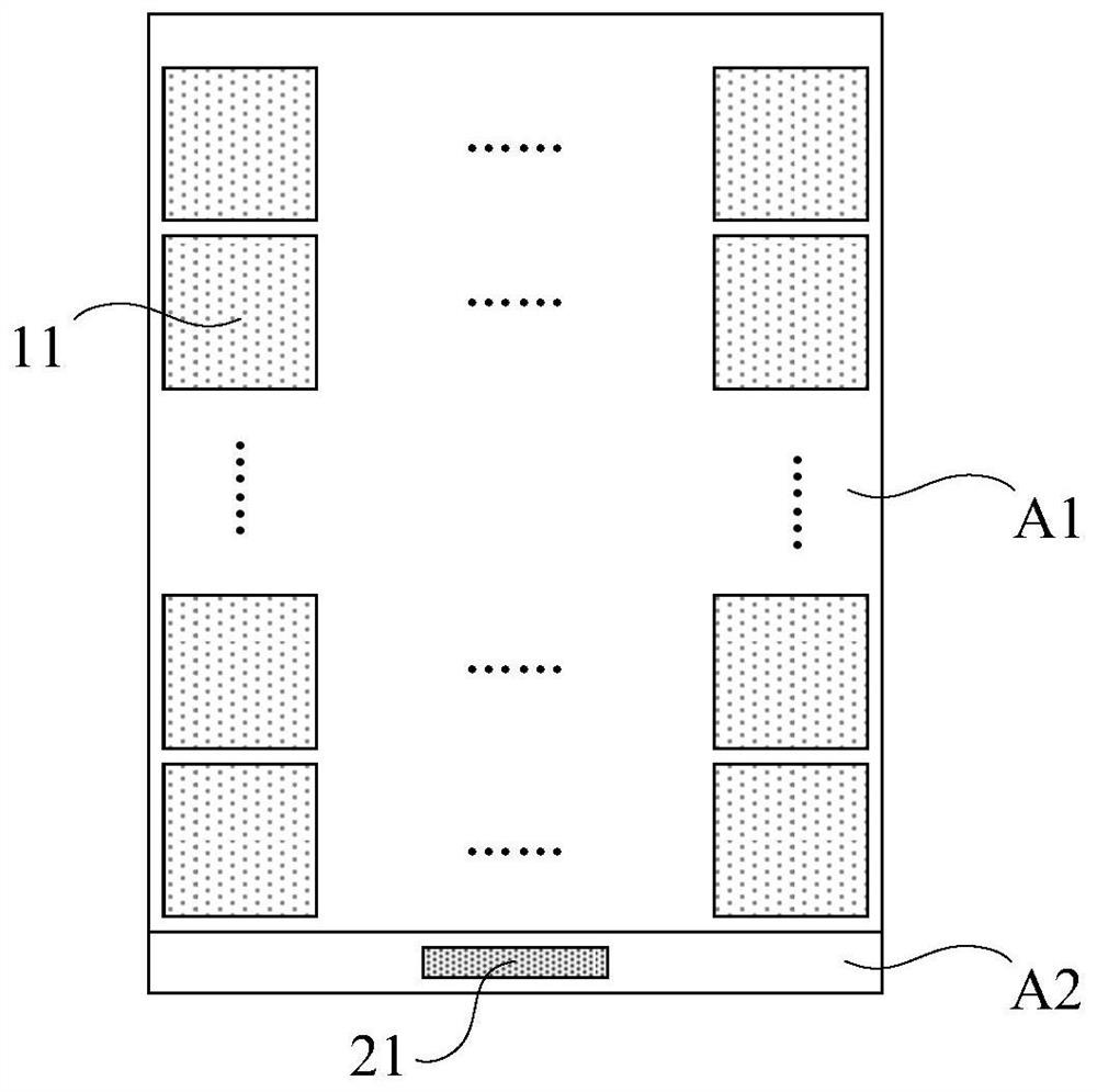
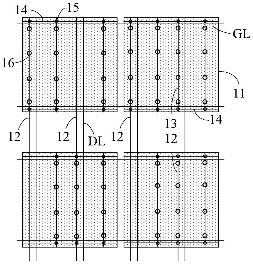
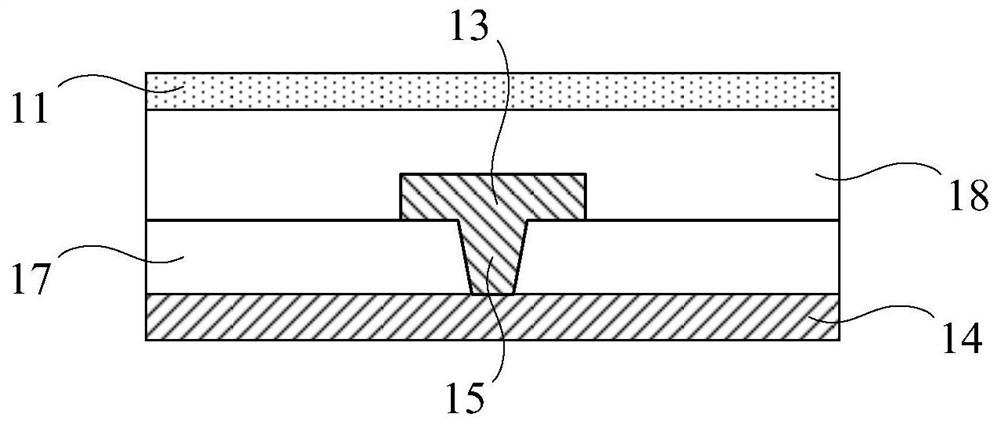
The disclosure provides an array substrate, a manufacturing method thereof, and a display device, which belong to the display field. The array substrate includes a display area and a peripheral circuit area, and the array substrate also includes: several touch electrodes located in the display area; several strips connecting the several touch electrodes to the peripheral circuit area Touch signal lines; a plurality of first conductor lines extending in the same direction as the plurality of touch signal lines; and a plurality of second conductor lines extending in a direction different from the plurality of touch signal lines; wherein, each The first conductor line is connected to the touch electrode in the thickness direction of one touch electrode; each second conductor line corresponds to a touch electrode, and any second conductor line is connected to the corresponding touch electrode. The touch signal line connected to the control electrode, and any second conductor line is respectively connected to each first conductor line connected to the corresponding touch electrode. The disclosure helps to improve the signal strength of the touch signal received by the substrate.

Description

technical field [0001] The present disclosure relates to the display field, and in particular to an array substrate, a manufacturing method thereof, and a display device. Background technique [0002] In touch products such as touch and display driver integration (Touch and Display driver Integration, TDDI), it is easy to generate touch due to the excessive resistance of the transparent touch electrode and the low signal strength of the received touch signal. Poor control. For example, touch electrodes covering a display area of ​​5×5 mm generally need to export the collected touch signals to external chips through metal leads, because the number of metal leads cannot be densely arranged due to the limitation of the aperture ratio, and the distance between the touch electrodes The touch signal generated at a relatively distant position of the metal lead will have considerable signal attenuation during transmission, so there is a problem that the local touch signal is easily...

Claims


Application Information

Patent Timeline
Patent Type & Authority Patents(China)
IPC IPC(8): G06F3/041H01L27/12H01L21/77
CPCH01L27/124H01L27/1259G06F3/0412G06F2203/04103G06F3/04164H01L27/1244G06F3/0443
Inventor 武新国王凤国史大为刘弘王子峰李峰马波郭志轩李元博段岑鸿赵晶
Owner BOE TECH GRP CO LTD
Why Eureka
Try Eureka