Chip strip type rigid framework-based chip packaging structure and process thereof

A chip packaging structure and rigid frame technology, applied in electrical components, electrical solid devices, circuits, etc., can solve the problems of low processing efficiency and unfavorable chip mass production, so as to improve work performance, improve processing efficiency and output, and improve heat generation. Effect

Inactive Publication Date: 2018-09-04
太极半导体(苏州)有限公司
View PDF6 Cites 1 Cited by
  • Summary
  • Abstract
  • Description
  • Claims
  • Application Information

AI Technical Summary

Problems solved by technology

[0004] In the existing packaging structure and process, the chip is flipped and filled with glue first, and after slicing, each chip packaging unit is assembled with a heat dissipation cover or a heat dissipation ring component, or a heat-conducting resin is packaged; resulting in low processing efficiency, which is not conducive to Mass production of chip packaging

Method used


Image

  • Chip strip type rigid framework-based chip packaging structure and process thereof
  • Chip strip type rigid framework-based chip packaging structure and process thereof
  • Chip strip type rigid framework-based chip packaging structure and process thereof

Examples


Embodiment Construction

[0026] The present invention is described below in conjunction with accompanying drawing.

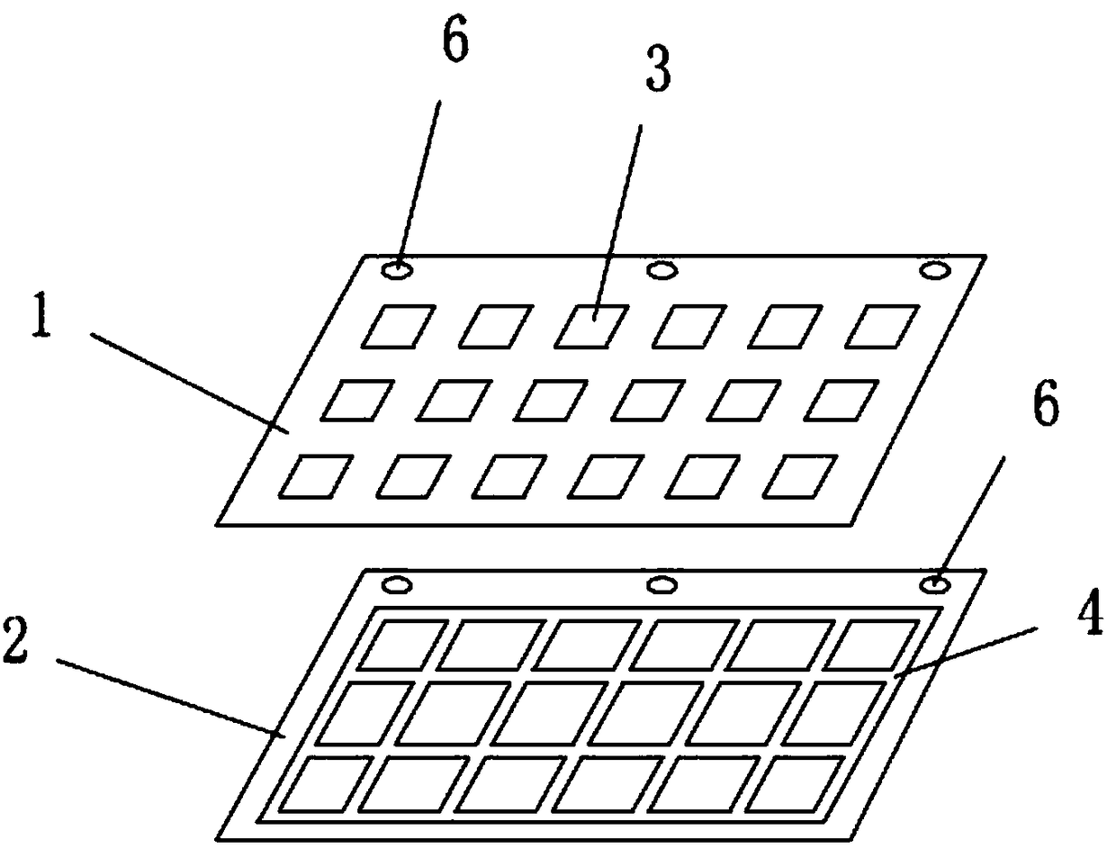
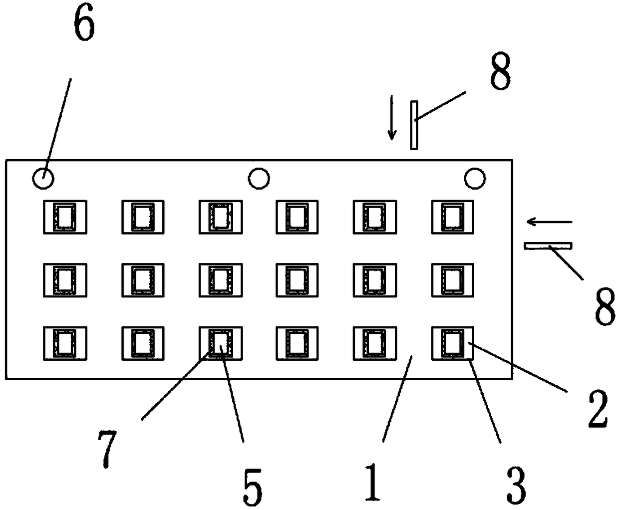
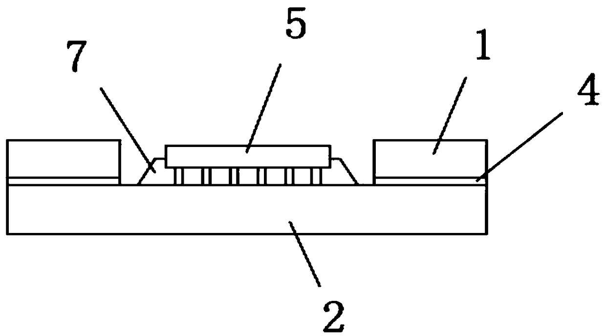
[0027] as attached Figure 1-2 As shown, a chip packaging structure based on a strip-type rigid frame according to the present invention includes a rigid frame 1 and a chip packaging substrate 2, and both the rigid frame 1 and the chip packaging substrate 2 are elongated sheet structures; The rigid frame 1 is provided with a plurality of uniformly arranged chip mounting holes 3, the chip packaging substrate 2 is provided with an adhesive layer 4, and the rigid frame 1 and the chip packaging substrate 2 are provided with a plurality of corresponding positioning holes 6, The rigid frame 1 and the chip packaging substrate 2 are positioned and aligned through the positioning holes 6, and are bonded through the adhesive layer 4; the adhesive layer 4 is a mesh structure, and the vacated part of the mesh structure corresponds to each chip mounting hole 3 , so that the adhesive layer 4 avoids ...


PUM


Abstract

The invention discloses a chip strip type rigid framework-based chip packaging structure and a process thereof. The chip packaging structure comprises a rigid framework and a chip packaging substrate;a chip mounting hole is formed in the rigid framework; an adhesive layer is arranged on the chip packaging substrate; the rigid framework is glued with the chip packaging substrate through the adhesive layer; a bare chip is arranged on the chip packaging substrate; the process comprises the steps of performing chip preprocessing, gumming, laminating, residual adhesive removal, bare chip pasting,reflow soldering, plasma cleaning, bottom filling with epoxy resin, and after completion, removing the residual adhesive and performing chip cutting. According to the process, after the rigid framework and the chip packaging substrate are integrally laminated, the bare chip is mounted, and then the integrated body is subjected to slicing and cutting to form each chip packaging unit, so that the warping problem in the conventional resin packaging is solved effectively, heating of the chip is relieved, and the working performance of the chip is improved; and in addition, one-by-one processing ofthe chip packaging units is avoided, so that the processing efficiency and yield of chip packaging are highly improved.

Description

technical field [0001] The invention relates to the technical field of chip packaging, in particular to a chip packaging structure and technology based on a strip type rigid frame. Background technique [0002] At present, the assembly of flip-chip products generally has the following forms: single-chip flip-chip array packaging with bottom filling, and can be matched with a single heat sink or cooling ring; strip flip-chip array packaging with bottom filling, and It can be packaged with thermally conductive resin, or strip-shaped flip-chip array package can be directly matched with thermally conductive resin package. [0003] The existing packaging process generally includes the following steps, wafer image quality evaluation, sticking tape, back grinding, wafer placement, sending to laser or mechanical dicing machine for dicing, secondary inspection, and then chip placement and reflow soldering , Plasma cleaning, bottom filling, and residual adhesive removal. After comple...

Claims


Application Information

Patent Timeline
Patent Type & Authority Applications(China)
IPC IPC(8): H01L23/31H01L21/56
CPCH01L21/56H01L23/31
Inventor 马军张光明杨健刘鹏
Owner 太极半导体(苏州)有限公司
Why Eureka
Try Eureka