Printed circuit board (PCB) detection device and method

A printed circuit board and testing device technology, applied in printed circuit testing, measuring devices, electronic circuit testing, etc., can solve problems such as lack of real-time detection of PCB boards, abnormal environmental protection processing, and inability to manage and control voltage, current, and temperature.

Active Publication Date: 2018-09-07
RIGOL
View PDF8 Cites 15 Cited by
  • Summary
  • Abstract
  • Description
  • Claims
  • Application Information

AI Technical Summary

Problems solved by technology

[0005] Embodiments of the present invention provide a detection device and method for a printed circuit board to solve the problem that the existing technology cannot manage and control the voltage, cur

Method used


Image

  • Printed circuit board (PCB) detection device and method
  • Printed circuit board (PCB) detection device and method
  • Printed circuit board (PCB) detection device and method

Examples


Embodiment Construction

[0055] The following will clearly and completely describe the technical solutions in the embodiments of the present invention with reference to the accompanying drawings in the embodiments of the present invention. Obviously, the described embodiments are only some, not all, embodiments of the present invention. Based on the embodiments of the present invention, all other embodiments obtained by persons of ordinary skill in the art without making creative efforts belong to the protection scope of the present invention.

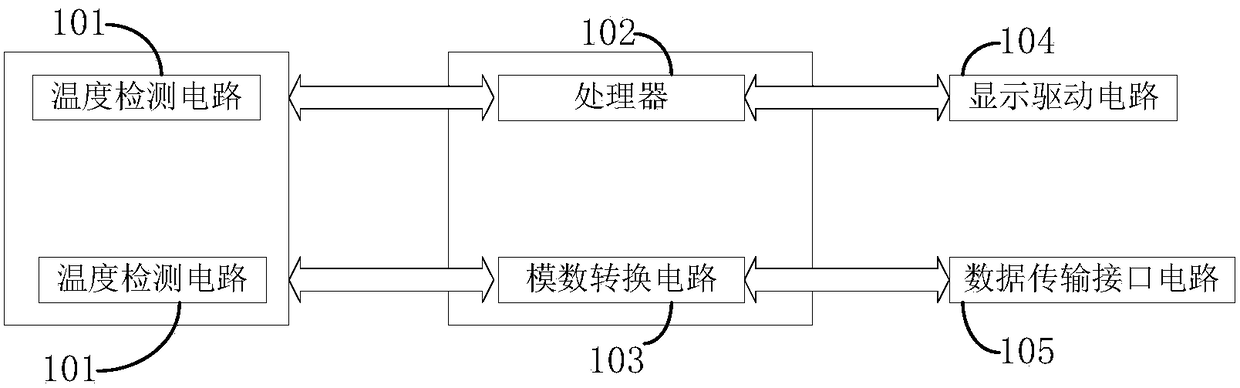
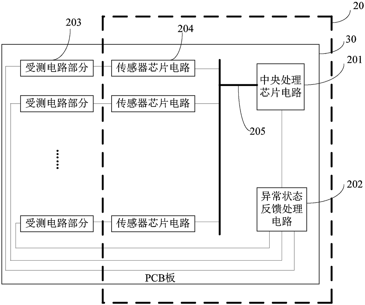
[0056] Such as figure 2 As shown, the embodiment of the present invention provides a detection device 20 for a printed circuit board, including: a central processing chip circuit 201, an abnormal state feedback processing circuit 202, and a plurality of sensor chips distributed in each tested circuit part 203 of the PCB board 30 circuit 204; the plurality of sensor chip circuits 204 are respectively connected to the central processing chip circuit 201; the ce...


PUM


Abstract

The invention provides a PCB detection device and method, and relates to the technical field of PCB detection. The device comprises a central processing chip circuit, an abnormal state feedback processing circuit and sensor chip circuits arranged in different tested circuit parts of a PCB. In each sensor chip circuit, a temperature detection circuit, a voltage detection circuit and a current detection circuit are integrated; the sensor chip circuits detect operation parameters of the different tested circuit parts of the PCB; the central processing chip circuit determines whether the operationparameters are abnormal; and the abnormal state feedback processing circuit selects a preset feedback processing strategy according to the abnormal operation parameter, and controls and processes thetested circuit part, corresponding to the abnormal operation parameter, of the PCB according to the preset feedback processing strategy. Thus, automatic detection and closed-loop response processingcan be realized for the whole system.

Description

technical field [0001] The invention relates to the technical field of detection of printed circuit boards, in particular to a detection device and method for printed circuit boards. Background technique [0002] With the gradual popularization of technologies such as electronic circuits and communication networks, printed circuit boards (Printed circuit boards, referred to as PCB boards) have been widely used in the field of electronic circuits, such as computers, medical equipment, and various electronic measuring instruments. It needs to be applied to the PCB board. For example, a spectrum analyzer is a very precise electronic measuring instrument, which is mainly used in base station maintenance, electronic product research and development, production and other fields. In various application fields, spectrum analyzers have high requirements for system stability, reliability, and consistency. For some precision electronic measuring instruments such as spectrum analyzers...

Claims


Application Information

Patent Timeline
IPC IPC(8): G01R31/28
CPCG01R31/2801G01R31/2806G01R31/281Y02D10/00
Inventor 张雨田秦喜朋王悦王铁军李维森
Owner RIGOL
Why Eureka
Try Eureka