Semiconductor device

一种半导体、导电层的技术,应用在半导体器件、半导体/固态器件零部件、晶体管等方向,能够解决不能元件施加偏置电压等问题,达到确保电接触、成品率提高的效果

Active Publication Date: 2018-09-07
MURATA MFG CO LTD
View PDF2 Cites 0 Cited by
  • Summary
  • Abstract
  • Description
  • Claims
  • Application Information

AI Technical Summary

Problems solved by technology

Furthermore, the above-mentioned conventional semiconductor device disclosed in Patent Document 2 suppresses the diffusion of the metal component only to the surface of the upper electrode, rather than suppressing the diffusion of the metal component to the insulating film in the region adjacent to the electrode.
In addition, although a TiNO layer is used as the diffusion barrier layer of Al, since the TiNO layer forms an insulating film, it is considered that if it is inserted into the electrode layer, the bias voltage cannot be effectively applied to the device.

Method used


Image

  • Semiconductor device
  • Semiconductor device
  • Semiconductor device

Examples


Embodiment Construction

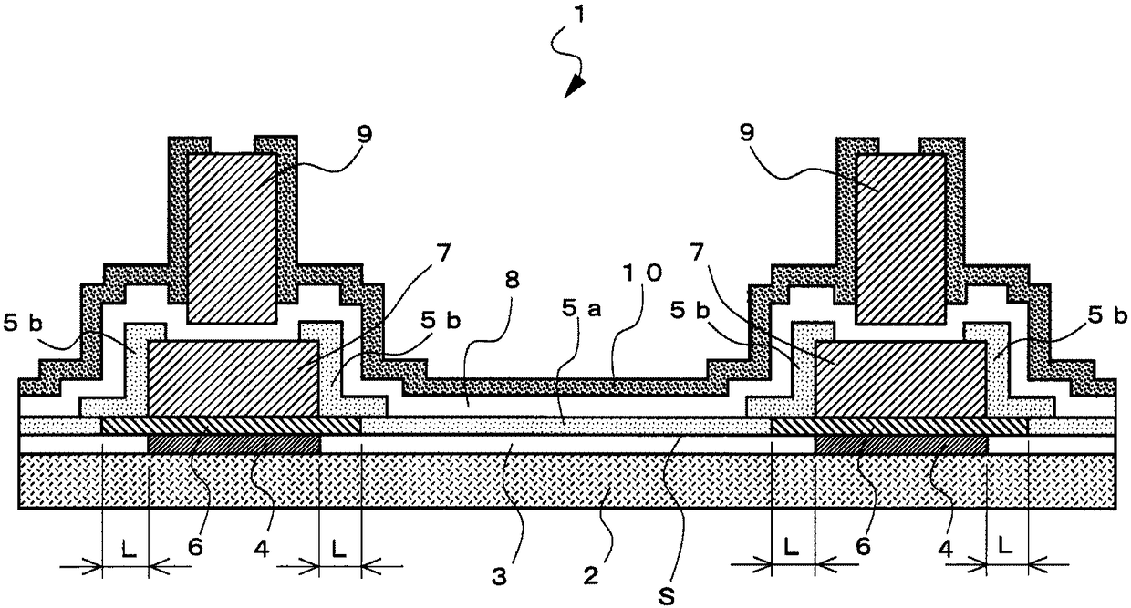
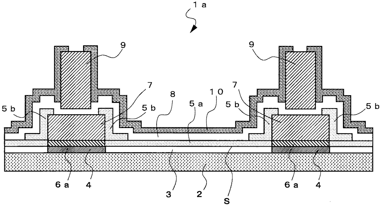
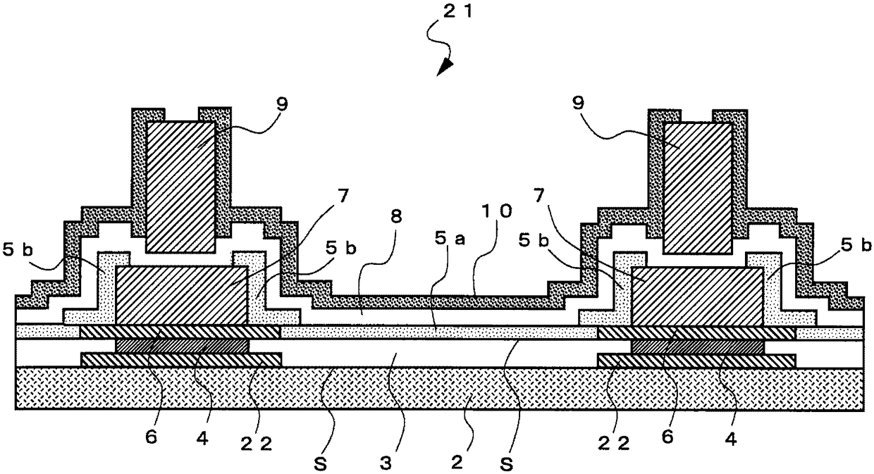
[0050] Next, an embodiment of a semiconductor device for implementing the present invention will be described.

[0051] figure 1 It is a cross-sectional view of the semiconductor device 1 according to the first embodiment of the present invention.

[0052] The semiconductor device 1 is formed on a GaAs semiconductor substrate 2 , and the first via layer 3 is selectively removed on the surface of the GaAs semiconductor substrate 2 to form conductive layers 4 , 4 . The first via layer 3 is formed from silicon nitride (silicon nitride: Si 3 N 4 ) composed of insulating film. A via hole is formed in the first via layer 3 , and a conductive material for connecting the upper layer wiring and the lower layer wiring is filled in the via hole groove, thereby forming a via hole. The conductive layers 4 and 4 are composed of metal electrodes, and serve as collector electrodes composed of Au when the semiconductor device 1 is formed of, for example, a heterojunction bipolar transistor...


PUM


Abstract

The invention provides a semiconductor device capable of suppressing the occurrence of such a migration of an electrode component of Au, ensuring the electrical contact between the electrode and a conductive layer under the electrode well, and having an increased yield. The semiconductor device includes electrodes which contain Au and which are placed above conductive layers in a region adjacent to stacked insulating films and also includes base layers which are composed of compositionally modulated layers and which are placed between the electrodes and the conductive layers. The base layers include lateral end sections composed of single layers projecting from lateral end sections of the electrodes in the direction of the interlayer interface between the insulating films; sections which are located under the electrodes and of which a major compositional component is Ti or Ti and W; and projecting sections which project from under the electrodes in the direction of the interlayer interface between the insulating films and of which compositional components are compositionally modulated to Ti and O, to Ti, O, and N, or to Ti, W, O, and N.

Description

technical field [0001] The present invention relates to a semiconductor device in which an electrode containing Au is formed on a conductive layer in a region adjacent to a stacked insulating film, and more particularly to a semiconductor device having a structure that restricts migration of a metal component forming the electrode. Background technique [0002] Conventionally, as a semiconductor device that restricts such migration, there is, for example, a semiconductor device disclosed in Patent Document 1 that has a structure that restricts migration of Cu, a metal component that forms wiring electrodes. In this semiconductor device, a first wiring layer is formed on a substrate surface of a semiconductor substrate. The first wiring layer includes an interlayer insulating film, a side barrier metal layer, Cu wiring, and an upper surface barrier metal layer. The upper surface portion of the Cu wiring is covered with an upper surface barrier metal layer formed of the same ...

Claims


Application Information

Patent Timeline
Patent Type & Authority Applications(China)
IPC IPC(8): H01L29/73H01L29/45H01L49/02
CPCH01L28/75H01L29/452H01L29/73H01L23/485H01L23/53252
Inventor 佐野雄一黑川敦小林一也
Owner MURATA MFG CO LTD
Why Eureka
Try Eureka