Packaging method and packaging structure of piezoelectric acoustic wave device

A packaging method and piezoelectric acoustic wave technology, applied in the direction of electrical components, impedance networks, etc., can solve the problems of instability in the effective active area of ​​piezoelectric acoustic wave devices, deterioration of device performance, etc., and achieve high packaging yield, better stability, and Good stability effect

Active Publication Date: 2018-09-07
SUZHOU HUNTERSUN ELECTRONICS CO LTD
View PDF6 Cites 22 Cited by
  • Summary
  • Abstract
  • Description
  • Claims
  • Application Information

AI Technical Summary

Problems solved by technology

However, due to the limitations of the existing technology, there will inevitably be a gap between the effective active area of ​​the piezoelectric acoustic wave device and the sealing wall, so a small amount of sealing material will still pass through the sealing wall during the formation of the sealed shell. Gaps into the inside of the seal wall
If the sealing material entering the inner side of the sealing wall comes into contact with the active active area of ​​the piezoelectric acoustic wave device, it will lead to the deterioration of the performance of the device
That is to say, since the method of forming a sealing wall on the substrate in the prior art cannot completely avoid the contact between the sealing material and the effective active area of ​​the piezoelectric acoustic wave device, the packaging of the piezoelectric acoustic wave device in this way still has a negative impact on the piezoelectric acoustic wave device. Potential for Instabilities Caused by the Active Active Region of Acoustic Devices

Method used


Image

  • Packaging method and packaging structure of piezoelectric acoustic wave device
  • Packaging method and packaging structure of piezoelectric acoustic wave device
  • Packaging method and packaging structure of piezoelectric acoustic wave device

Examples


Embodiment Construction

[0055] In order to better understand and illustrate the present invention, the present invention will be further described in detail below in conjunction with the accompanying drawings.

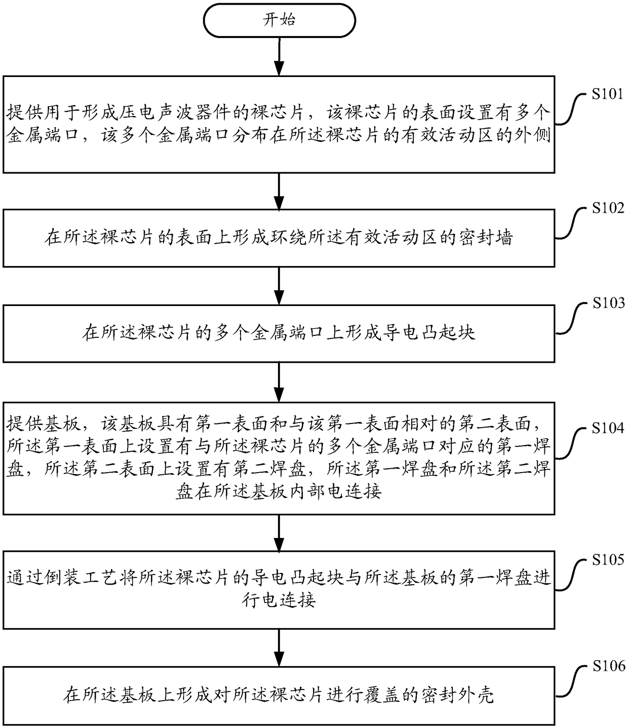
[0056] The invention provides a packaging method for a piezoelectric acoustic wave device. Please refer to figure 1 , figure 1 It is a flowchart of a packaging method for a piezoelectric acoustic wave device according to a specific embodiment of the present invention. As shown, the encapsulation method includes:

[0057] In step S101, a bare chip for forming a piezoelectric acoustic wave device is provided, the surface of the bare chip is provided with a plurality of metal ports, and the plurality of metal ports are distributed outside the effective active area of ​​the bare chip;

[0058] In step S102, a sealing wall surrounding the effective active area is formed on the surface of the bare chip;

[0059] In step S103, forming conductive bumps on multiple metal ports of the bare chip;

...


PUM


Abstract

The invention provides a packaging method of a piezoelectric acoustic wave device. The packaging method comprises the following steps: providing a bare chip, wherein multiple metal ports are arrangedon the surface of the bare chip, and the multiple metal ports are distributed on the outer side of an effective active region of the bare chip; forming a sealing wall surrounding the effective activeregion on the surface of the bare chip; forming conductive convex blocks on the multiple metal ports of the bare chip; providing a base plate, wherein a first welding pad corresponding to the multiplemetal ports of the bare chip is arranged on one surface of the base plate, and a second welding pad is arranged on the other surface of the base plate; electrically connecting the conductive convex blocks of the bare chip with the first welding pad of the base plate through the flip-chip process; and forming a sealing outer shell, covering the bare chip, on the base plate. Correspondingly, the invention further provides a packaging structure of the piezoelectric acoustic wave device. By implementation of the packaging method of the piezoelectric acoustic wave device and the packing structureof the piezoelectric acoustic wave device, the instability of a traditional sealing process is transferred to the surface of the base plate, so that the effective active region of the piezoelectric acoustic wave device is effectively protected.

Description

technical field [0001] The invention relates to the technical field of semiconductor packaging, in particular to a packaging method and packaging structure of a piezoelectric acoustic wave device. Background technique [0002] In communication and other electrical fields, piezoelectric acoustic wave devices are frequently used as radio frequency and intermediate frequency filters to achieve frequency selection and other electrical functions due to their small size, excellent performance, and suitability for mass production. The work of piezoelectric acoustic wave devices depends on the excitation, transmission and conversion of acoustic waves, including surface acoustic waves and bulk acoustic waves. When the piezoelectric acoustic wave device works, the acoustic wave is transmitted along or very close to the surface of the piezoelectric material, or in its body. Among them, the effective area where the electric energy-sound energy-electrical energy conversion is realized i...

Claims


Application Information

Patent Timeline
Patent Type & Authority Applications(China)
IPC IPC(8): H03H9/10H03H9/17H03H9/54H03H9/64H03H3/08H03H3/02
CPCH03H3/02H03H3/08H03H9/1042H03H9/1064H03H9/17H03H9/54H03H9/64
Inventor 田晓洁赖亚明谢恒赖志国蔡洵
Owner SUZHOU HUNTERSUN ELECTRONICS CO LTD
Why Eureka
Try Eureka