Unlock instant, AI-driven research and patent intelligence for your innovation.

Superlarge area array CMOS image sensor structure

An image sensor and area array technology, which is applied in the field of super large area array CMOS image sensor structure to achieve the effect of high-speed readout technology

Active Publication Date: 2018-09-11
XIAN MICROELECTRONICS TECH INST
View PDF5 Cites 9 Cited by
  • Summary
  • Abstract
  • Description
  • Claims
  • Application Information

AI Technical Summary

Problems solved by technology

In the layout design, it is only limited by the column width in the vertical direction, and it is easier to design
However, it is still unable to solve the noise and speed problems of the super large area array.

Method used


Image

  • Superlarge area array CMOS image sensor structure
  • Superlarge area array CMOS image sensor structure
  • Superlarge area array CMOS image sensor structure

Examples


Embodiment Construction

[0031] The present invention will be further described in detail below in conjunction with specific embodiments, which are explanations of the present invention rather than limitations.

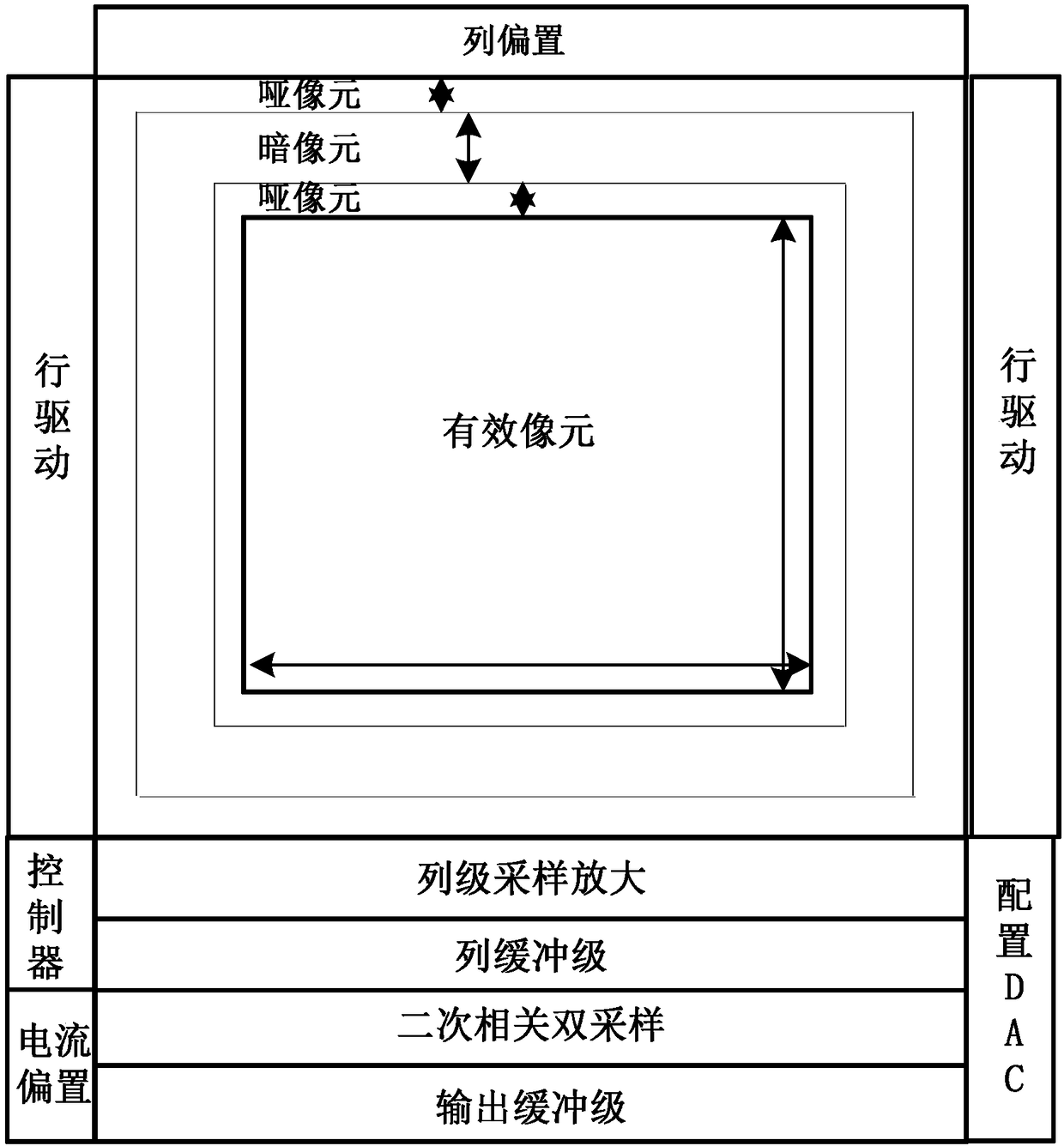
[0032] The present invention is a super large area array CMOS image sensor structure, including photosensitive area array, row drive, column bias, column level sampling amplification module, column buffer level, second level correlated double sampling module, output buffer level, controller, current bias and configurable DAC. The row drive of the photosensitive surface array is composed of left and right sides, and is realized by the matching mode of the left and right sides; the column-level sampling amplification module and the column bias module of the photosensitive surface array are placed on the upper and lower sides of the photosensitive surface array, and the photosensitive surface array The pixel bias is provided by the column bias located above the area array, and the readout circui...


PUM


Abstract

The invention discloses a superlarge area array CMOS image sensor structure comprising a photosensitive area array, row drives, a column bias, a read circuit, a controller, a current bias and a configurable DAC, wherein the drive of the photosensitive area array comprises the row drives separately arranged on left and right sides, the column bias used for providing pixel element biasing is arranged on the upper side of the photosensitive area array, and the read circuit is arranged on the lower side of the same; the read circuit comprises a column stage read circuit and an output stage read circuit; the controller is applied to sequential control of exposing, converting, sampling, amplification and read operations, and also used for cooperatively controlling the photosensitive area array and the read circuit and configuring exposure time and DAC; the current bias is used for transmitting current bias signals in the whole system, and the current bias signals comprise the output signalsof the column bias, configurable DAC, column stage read circuit and output stage read circuit; and the configurable DAC is used for correcting the column stage read circuit and output stage read circuit. Therefore, the affect of the post-stage read circuit on the system noise is reduced.

Description

technical field [0001] The invention relates to a CMOS image sensor, in particular to a super large area array CMOS image sensor structure. Background technique [0002] CMOS image sensors are widely used in the field of image acquisition due to their low power consumption, small size, and low price. Commonly used CMOS visible light image sensor processing systems can be divided into three different types according to their architectures: pixel-level processing systems, column-level processing systems, and chip-level processing systems. [0003] The pixel-level processing system refers to that each pixel unit or every few pixel units in the image sensor pixel array share a readout circuit, so that a two-dimensional array of readout circuits is integrated in an image sensor. This processing system has many important advantages, including parallel processing, high signal-to-noise ratio, and low power consumption. In addition, this structure requires the minimum speed of the ...

Claims


Application Information

Patent Timeline
IPC IPC(8): H04N5/374H04N5/357
CPCH04N25/60H04N25/76
Inventor 郭仲杰汪西虎吴龙胜
Owner XIAN MICROELECTRONICS TECH INST