Eureka AIR delivers breakthrough ideas for toughest innovation challenges, trusted by R&D personnel around the world.

Display substrate and display device

A technology of display substrate and pixel grid, which can be used in measurement devices, instruments, X/γ/cosmic radiation measurement, etc., and can solve problems such as large-area grayscale abnormalities in display devices

Pending Publication Date: 2018-09-14
BOE TECH GRP CO LTD +1
View PDF0 Cites 0 Cited by
  • Summary
  • Abstract
  • Description
  • Claims
  • Application Information

AI Technical Summary

Problems solved by technology

[0005] In order to overcome the technical problems and defects of the large-area gray scale of the display device caused by the alignment shift between the TFT layers in the actual process production, the application provides a display substrate and a display device to solve the problems existing in the prior art. The display device is prone to the technical problem of large-area gray scale abnormality

Method used


Image

  • Display substrate and display device
  • Display substrate and display device
  • Display substrate and display device

Examples


Embodiment Construction

[0033] Before introducing this application, let me briefly introduce the devices and working principles related to the thin film transistor TFT.

[0034] The TFT liquid crystal display is mainly composed of three parts: the rear panel module, the liquid crystal layer and the front panel module.

[0035] The rear panel module refers to the part behind the liquid crystal layer, which is mainly composed of a rear polarizing plate, a glass plate, a pixel unit (the pixel unit includes a pixel electrode, thin film transistor and other structures), and a rear alignment film. Each pixel unit includes multiple sub Pixel unit, such as: a pixel unit includes three primary colors of sub-pixel units; three primary colors of sub-pixel units include sub-pixel units with a red emission color, sub-pixel units with a green emission color, and sub-pixel units with a blue emission color. Pixel unit. It should be noted that the sub-pixels involved in this application may also be referred to as sub-pix...


PUM


Abstract

The invention provides a display substrate and a display device. The display substrate comprises a plurality of pixel grids, wherein a specific number of sub pixels are set in each pixel grid; each sub pixel is correspondingly provided with a thin film transistor (TFT); and in each pixel grid, at least two TFTs are symmetric along the geometric center of the pixel grid. By change of a TFT arrangement mode design of a glass panel, the TFTs in the pixel grids are not totally arranged at the same positions of the corresponding sub pixels, variations of parasitic capacitors of the TFTs can compensate one other to a certain degree, and the variations of the parasitic capacitors of the TFTs in the whole pixel grids are reduced greatly; and thus, large-area blackening or whitening of the displaysubstrate is avoided macroscopically, and meanwhile, a display result is uniform visually.

Description

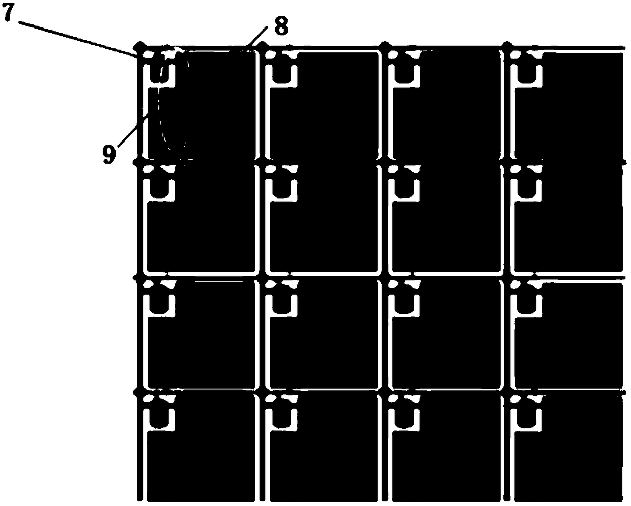
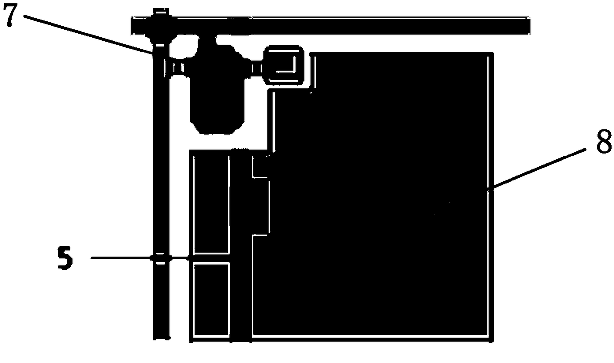
Technical field [0001] The present application relates to the field of display technology. Specifically, the present application relates to a display substrate and a display device. Background technique [0002] There are many display devices used for display functions in daily life, such as display screens, display panels, and so on. If some display devices are used in the industrial field, the user can view the internal structure of the electronic accessories through the display device; if they are used in the medical field, the user can view the disease inside the patient's body through the display device. It can be seen that the performance of the display device is directly related to many aspects of people's work and life. [0003] Attached figure 1 It is an arrangement of thin film transistors TFT on the glass panel of a display device in the prior art, with figure 1 The middle number 7 represents TFT (Thin Film Transistor, thin film transistor), the number 8 represents the ...

Claims


Application Information

Patent Timeline
Patent Type & Authority Applications(China)
IPC IPC(8): G02F1/1362G02F1/1368
CPCG02F1/1362G02F1/13624G02F1/1368H01L27/14663H10K59/1213G01T1/208H01L27/14603
Inventor 李阳恒刘弘李慧颖田雪
Owner BOE TECH GRP CO LTD
Why Eureka
Eureka Blog
Learn More