
Display panel and display device

A technology of display panel and substrate substrate, which is applied in recognition devices, static indicators, character and pattern recognition, etc., can solve the problems of sub-pixels stealing light, and achieve the effect of reducing capacitive coupling and improving image display effect.

Active Publication Date: 2018-09-28
WUHAN TIANMA MICRO ELECTRONICS CO LTD
View PDF7 Cites 36 Cited by
  • Summary
  • Abstract
  • Description
  • Claims
  • Application Information

AI Technical Summary

Problems solved by technology

[0004] The present invention provides a display panel and a display device, which can reduce the capacitive coupling between the scanning line and the metal anode, solve the problems of not being dark in the dark state and stealing the brightness of sub-pixels, and improve the display effect

Method used


Image

  • Display panel and display device
  • Display panel and display device
  • Display panel and display device

Examples


Embodiment Construction

[0024] The present invention will be further described in detail below in conjunction with the accompanying drawings and embodiments. It should be understood that the specific embodiments described here are only used to explain the present invention, but not to limit the present invention. In addition, it should be noted that, for the convenience of description, only some structures related to the present invention are shown in the drawings but not all structures.

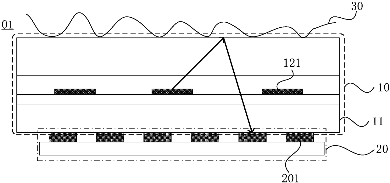
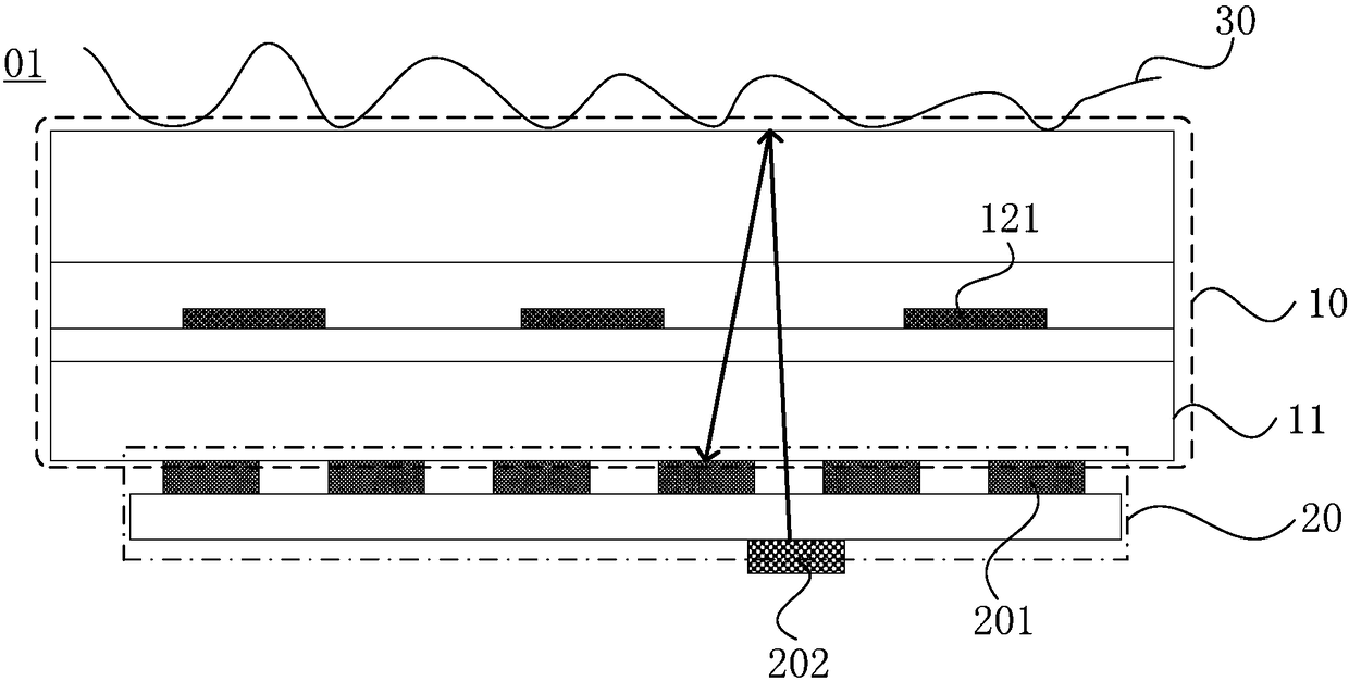
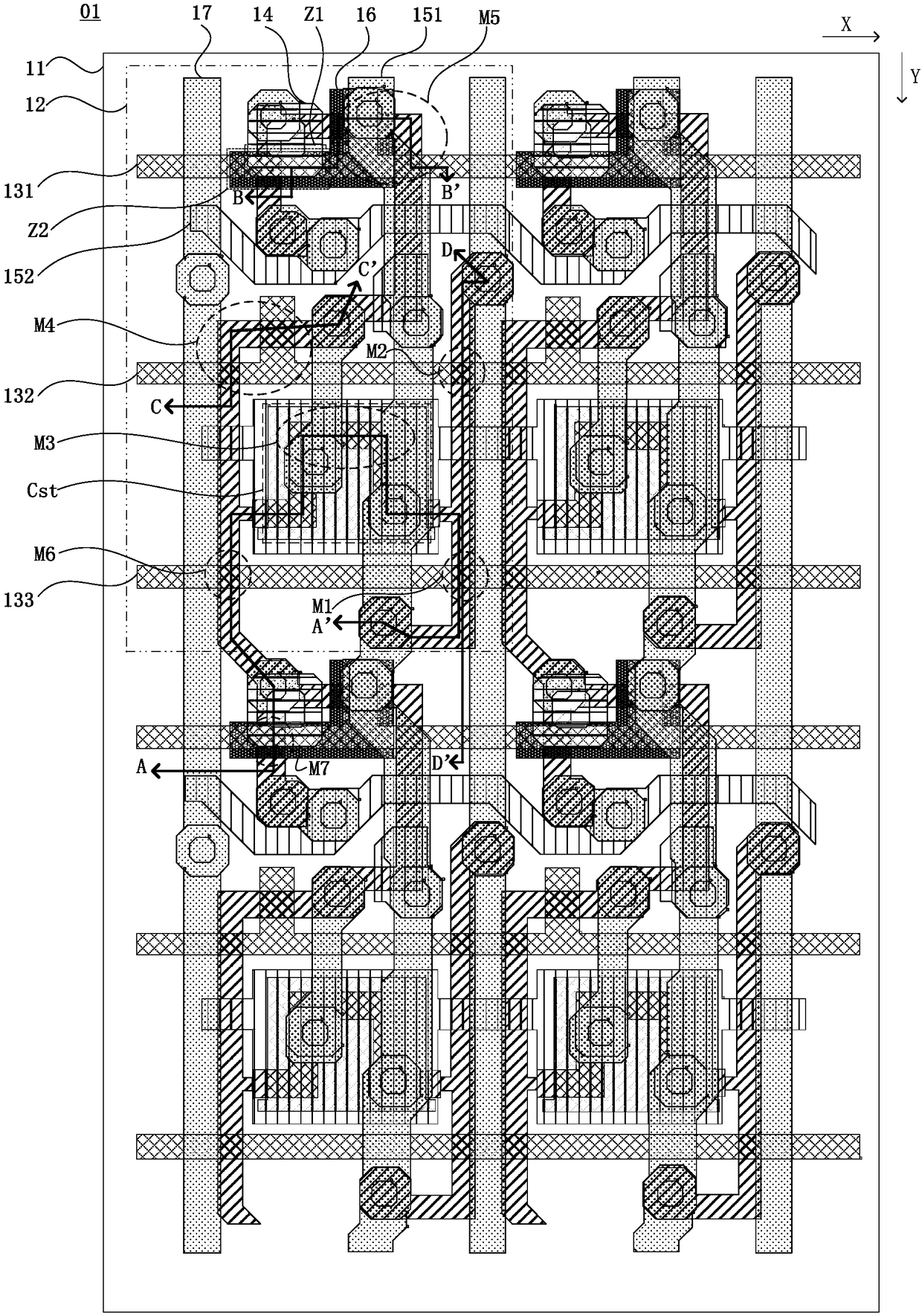
[0025] The display panel provided by the embodiment of the present invention has a fingerprint identification function, and can improve the capacitive coupling between the first scanning line and the metal anode, and improve the image display effect of the display panel. Specifically, the display panel includes a display module and a fingerprint identification module; the display module includes a base substrate, a plurality of pixel units located on one side of the base substrate, and a first scanning line extendi...


PUM


Abstract

The embodiment of the invention discloses a display panel and a display device. The display panel comprises a display module and a fingerprint identification module, wherein the display module comprises a substrate base plate, a plurality of pixel units positioned on one side of the substrate base plate, and first scanning lines extending along the first direction, each pixel unit comprises a pixel drive unit and a light-emitting unit positioned on the side, far away from the substrate base plate, of the pixel drive unit, and the light-emitting unit comprises a metal anode; the fingerprint identification module is used for carrying out fingerprint identification according to light rays reflected to a fingerprint identification unit through a touch main body; the vertical projection of thefirst scanning lines on the substrate base plate and the vertical projection of the metal anode on the substrate base plate have an overlapped area. For the display panel provided by the embodiment ofthe invention, shielding electrodes are arranged between the film layer where the first scanning lines are located and the film layer where drain electrodes are located, the shielding electrodes andthe drain electrodes are insulated, the vertical projection of the shielding electrodes on the substrate base plate and the overlapped area are overlapped, the capacity coupling between the metal anode and the first scanning lines can be reduced, and thus the image display effect is improved.

Description

technical field [0001] The present invention relates to display technology, in particular to a display panel and a display device. Background technique [0002] Each person's skin texture (including fingerprints) is different in patterns, breakpoints and intersections, which are unique and remain unchanged throughout life. Accordingly, we can match a person with his fingerprint, and verify his real identity by comparing his fingerprint with the pre-saved fingerprint data. This is fingerprint recognition technology. With the development of electronic integrated manufacturing technology, optical fingerprint recognition technology in fingerprint recognition technology has begun to enter our daily life, and has become the most in-depth research, the most widely used and the most mature technology in biometrics. [0003] At present, the optical fingerprint identification technology is usually combined with the display technology, so that the display panel not only has a normal d...

Claims


Application Information

Patent Timeline
Patent Type & Authority Applications(China)
IPC IPC(8): G09F9/30G09G3/20G06K9/00
CPCG09F9/30G09G3/20G06V40/1318G06F3/0421G06F3/0412G06F3/04166G06F2203/04103G06V40/1306G06V40/1376G06V10/17G06F3/044
Inventor 高娅娜周星耀李玥向东旭刘昕昭
Owner WUHAN TIANMA MICRO ELECTRONICS CO LTD
Learn More