Flat panel display apparatus

a flat panel display and display device technology, applied in the direction of screens, electric discharge tubes, semiconductor devices, etc., can solve the problems of increasing the manufacturing increasing the cost of the oled apparatus, and deteriorating so as to improve the image display quality of the flat panel display apparatus, reduce the thermal budget of the organic light emitting element, and improve the effect of the protection layer

Active Publication Date: 2006-06-29
SAMSUNG DISPLAY CO LTD
View PDF3 Cites 30 Cited by
  • Summary
  • Abstract
  • Description
  • Claims
  • Application Information

AI Technical Summary

Benefits of technology

[0010] The present invention provides a flat panel display apparatus capable of improving an image display quality and decreasing a manufacturing cost.
[0019] Therefore, the protecting layer of the flat panel display apparatus is formed using the auxiliary plate so that a thermal budget of the organic light emitting element is decreased. In addition, the protecting layer may be formed at a high temperature so that a permeability of the protecting layer is increased, thereby improving an image display quality of the flat panel display apparatus. Furthermore, the protecting layer may be formed under oxygen atmosphere so that a manufacturing cost of the flat panel display apparatus is decreased.
[0020] In addition, the flat panel display apparatus includes the organic buffer layer that has the inorganic insulation particles to protect the organic light emitting element from an impurity or an impact that is provided from an exterior to the organic light emitting element, thereby decreasing the thermal budget of the organic light emitting element.

Problems solved by technology

When the organic light emitting layer is in the closed space, a manufacturing process of the OLED apparatus is complicated, and the manufacturing cost of the OLED apparatus is increased.
In addition, when the protecting layer having the polymers is formed in a high temperature, a crack may be formed in the polymers.
When the inorganic layer is directly formed on the organic light emitting element, the organic light emitting element may be deteriorated by a heat generated from the deposition process.

Method used


Image

  • Flat panel display apparatus
  • Flat panel display apparatus
  • Flat panel display apparatus

Examples


Embodiment Construction

[0038] It should be understood that the exemplary embodiments of the present invention described below may be varied modified in many different ways without departing from the inventive principles disclosed herein, and the scope of the present invention is therefore not limited to these particular following embodiments. Rather, these embodiments are provided so that this disclosure will be through and complete, and will fully convey the concept of the invention to those skilled in the art by way of example and not of limitation.

[0039] Hereinafter, the present invention will be described in detail with reference to the accompanying drawings.

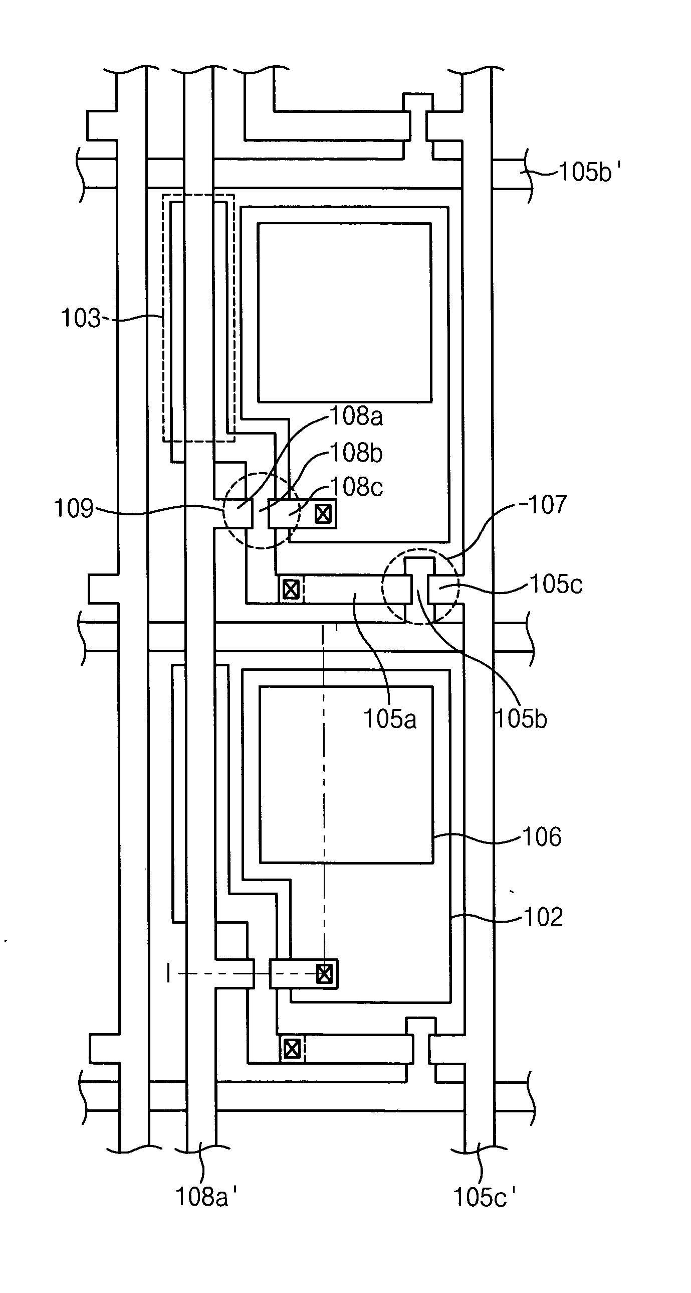
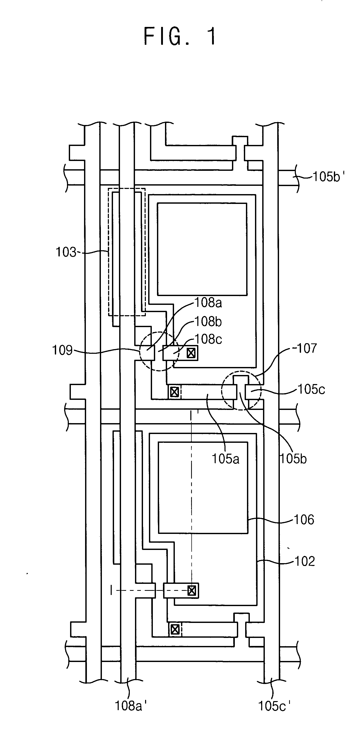
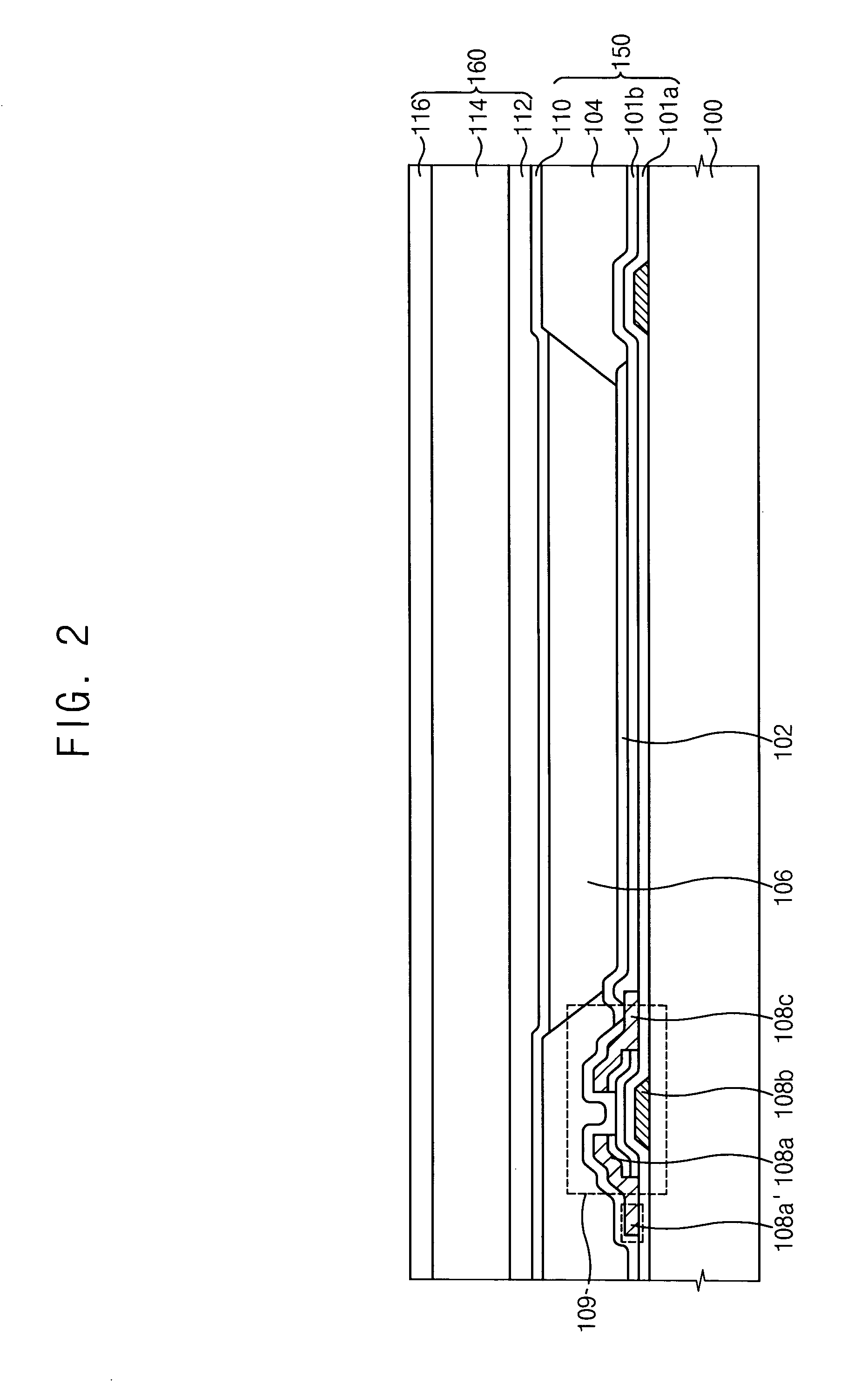
[0040]FIG. 1 is a plan view showing a flat panel display apparatus in accordance with an exemplary embodiment of the present invention. FIG. 2 is a cross-sectional view taken along the line I-I′ of FIG. 1.

[0041] Referring to FIGS. 1 and 2, the flat panel display apparatus includes a main plate 100, an organic light emitting element 150, a stora...


PUM


Abstract

A flat panel display apparatus includes a main plate, an organic light emitting element, a protecting layer and an attachable-detachable layer. The organic light emitting element includes a first electrode, a second electrode corresponding to the first electrode, and an organic light emitting layer disposed between the first and second electrodes to generate a light based on a current that flows between the first and second electrodes through the organic light emitting layer. The organic light emitting element is on the main plate. The protecting layer is on the organic light emitting element to protect the organic light emitting element. The attachable-detachable layer is on the protecting layer. Therefore, an image display quality is improved, and a manufacturing cost is decreased.

Description

TECHNICAL FIELD [0001] The present invention relates to a flat panel display apparatus and method of manufacturing the flat panel display apparatus. More particularly, the present invention relates to a flat panel display apparatus capable of improving an image display quality and decreasing a manufacturing cost and a method of manufacturing the flat panel display apparatus. BACKGROUND ART [0002] An organic light emitting element of an organic light emitting display (OLED) apparatus includes an anode, a cathode and an organic light emitting layer. Holes that are provided from the anode are combined with electrons that are provided from the cathode in the organic light emitting layer to generate exciton having excited state. When the exciton changes from an excitation state to a ground state, a light is generated from the light emitting layer. [0003] The OLED apparatus has various characteristics such as high luminance, wide viewing angle, thin thickness, low power consumption, etc. ...

Claims


Application Information

Patent Timeline
Patent Type & Authority Applications(United States)
IPC IPC(8): H01J31/48
CPCH01L27/3244H01L51/5253H10K59/12H10K50/844
Inventor KIM, HOONCHUNG, JAE-HOONCHOI, JOON-HOOLEE, SANG-PIL
Owner SAMSUNG DISPLAY CO LTD
Why Eureka
Try Eureka