Vertical cavity surface emitting laser and fabrication method thereof
A vertical cavity surface emission, laser technology, applied in the direction of lasers, laser components, semiconductor lasers, etc., can solve the problems of poor beam quality, widened laser line width, and restrictions on the application of large-aperture VCSELs
- Summary
- Abstract
- Description
- Claims
- Application Information
AI Technical Summary
Problems solved by technology
Method used
Image

Examples
Embodiment 2
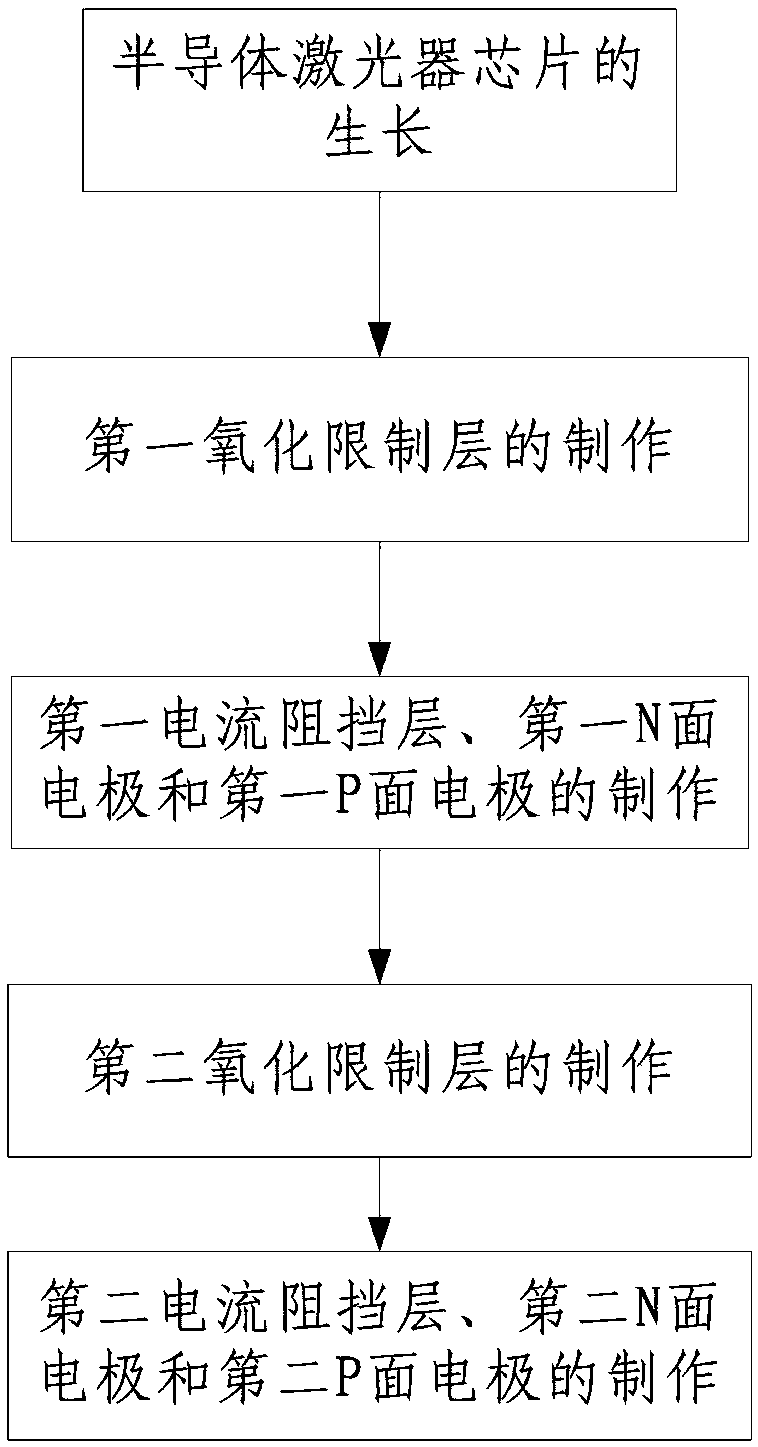
[0123] The preparation method comprises the following steps:
[0124] Step 1, the growth of the semiconductor laser chip:
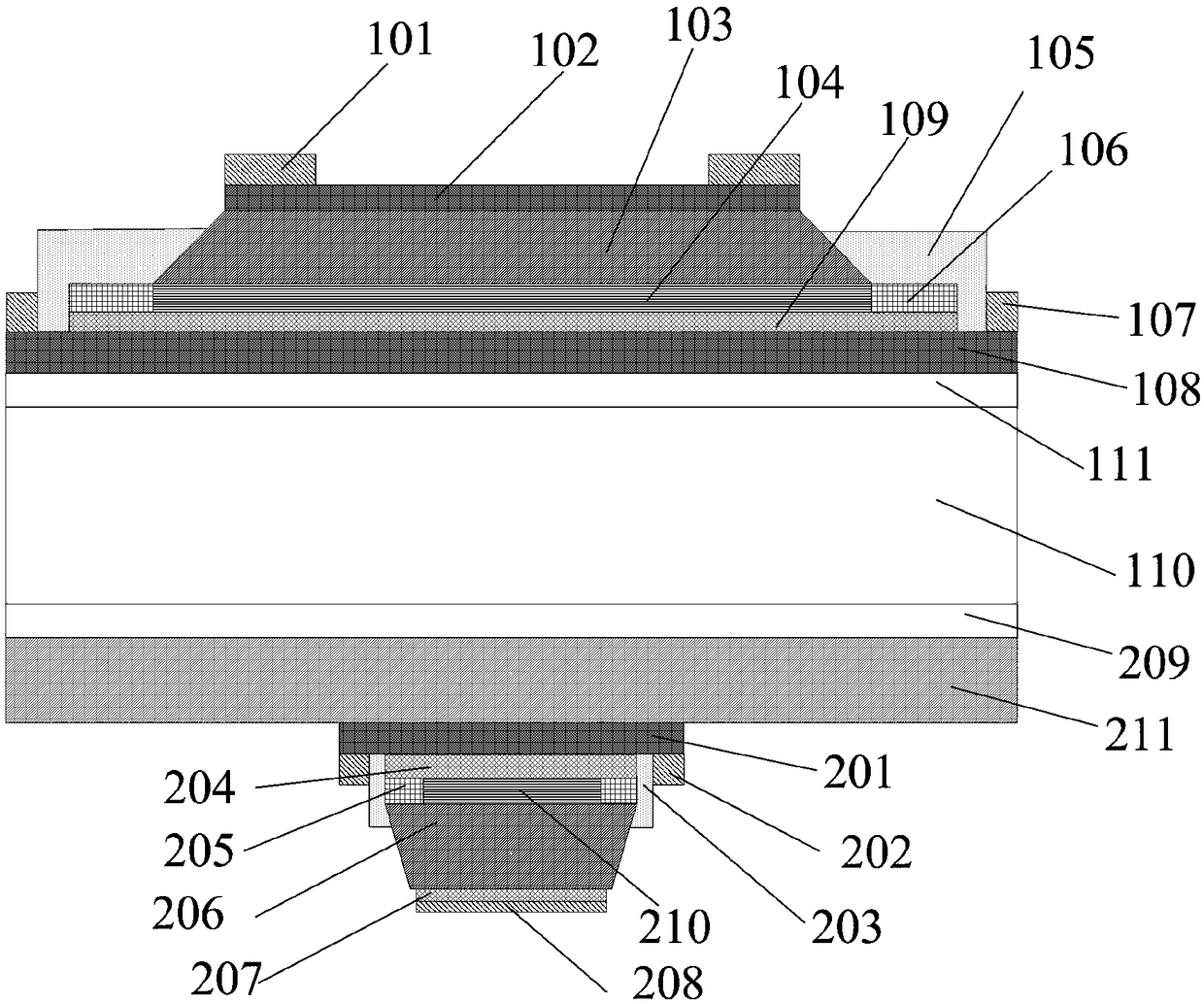
[0125] Step 101, selecting a semiconductor substrate 110; wherein, the thickness of the semiconductor substrate 110 is 150 μm;
[0126] Step 102, using a semiconductor growth method to epitaxially grow a first buffer layer 111 made of the same material as the semiconductor substrate 110 on the upper surface of the semiconductor substrate 110; wherein, the thickness of the first buffer layer 11 is 20 nm;
[0127] Step 103, using the semiconductor growth method to grow a first N-plane current guiding layer 108 with a thickness of 10 nm on the buffer layer 111;
[0128] Step 104, using the semiconductor growth method to grow a multi-period quantum well structure on the upper surface of the current guiding layer 108 to form the first active region 109; wherein, the period of the quantum well structure is 2 groups;
[0129] Step 105, using the semiconductor ...
Embodiment 3
[0192] The difference between the manufacturing method of the vertical cavity surface emitting laser of this embodiment and the second embodiment is only that:
[0193] In this embodiment, the thickness of the semiconductor substrate 110 in step 101 is 400 μm, the thickness of the first buffer layer 11 in step 102 is 2 μm, and the thickness of the first N-side current guiding layer 108 in step 103 is 50 nm, The period of the quantum well structure described in step 104 is 8 groups, the thickness of the first high aluminum layer 104 described in step 105 is 50nm, the period logarithm of the first refraction material layer described in step 106 is 26, in step 109 The period logarithm of the second refraction material layer is 32, and the period logarithm of the third refraction material layer in step 1013 is 38;
[0194] The thickness of the first passivation layer described in step 201 is 2 μm, the flow rate of nitrogen gas in step 203 is 2 L / min, and the time of wet oxidation ...
Embodiment 4
[0204] The difference between the manufacturing method of the vertical cavity surface emitting laser of this embodiment and the second embodiment is only that:
[0205] In this embodiment, the thickness of the semiconductor substrate 110 in step 101 is 275 μm, the thickness of the first buffer layer 11 in step 102 is 1.01 μm, and the thickness of the first N-side current guiding layer 108 in step 103 is 30 nm , the period of the quantum well structure described in step 104 is 5 groups, the thickness of the first high aluminum layer 104 described in step 105 is 30nm, the period logarithm of the first refraction material layer described in step 106 is 22, step 109 The period logarithm of the second refraction material layer in step 1013 is 29, and the period logarithm of the third refraction material layer in step 1013 is 32;
[0206] The thickness of the first passivation layer described in step 201 is 1.3 μm, the flow rate of nitrogen gas in step 203 is 1.5 L / min, and the wet ...
PUM
| Property | Measurement | Unit |
|---|---|---|
| Thickness | aaaaa | aaaaa |
| Thickness | aaaaa | aaaaa |
| Thickness | aaaaa | aaaaa |
Abstract
Description
Claims
Application Information
 - R&D Engineer
- R&D Manager
- IP Professional
- Industry Leading Data Capabilities
- Powerful AI technology
- Patent DNA Extraction
Browse by: Latest US Patents, China's latest patents, Technical Efficacy Thesaurus, Application Domain, Technology Topic.
© 2024 PatSnap. All rights reserved.Legal|Privacy policy|Modern Slavery Act Transparency Statement|Sitemap