PCB circuit board printing process and production line thereof

A PCB circuit board, circuit board technology, applied in the printing process, printing, printing machine, etc., can solve the problems of reduced production efficiency, long drying time, heat waste of the dryer, etc., to protect the PCB board, and the processing process is tight Coherent, fast processing effect

Active Publication Date: 2018-11-02
江西鑫金晖智能科技有限公司
View PDF5 Cites 19 Cited by
  • Summary
  • Abstract
  • Description
  • Claims
  • Application Information

AI Technical Summary

Problems solved by technology

This printing method can only dry one printed surface of the circuit board at a time, and the drying time i

Method used


Image

  • PCB circuit board printing process and production line thereof
  • PCB circuit board printing process and production line thereof
  • PCB circuit board printing process and production line thereof

Examples


Embodiment Construction

[0023] The following will clearly and completely describe the technical solutions in the embodiments of the present invention. Obviously, the described embodiments are only some of the embodiments of the present invention, rather than all the embodiments. Based on the embodiments of the present invention, all other embodiments obtained by persons of ordinary skill in the art without making creative efforts belong to the protection scope of the present invention.

[0024] Specific embodiments of the present invention will be described below in conjunction with the accompanying drawings.

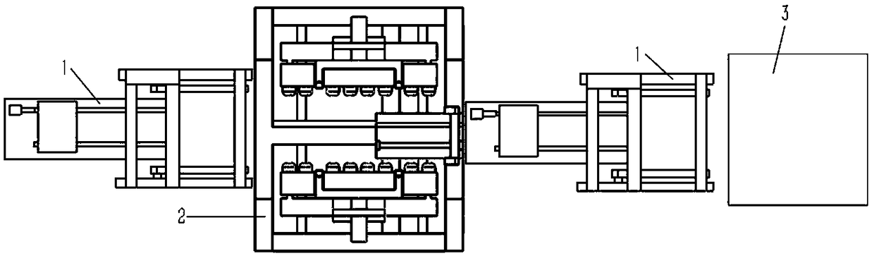
[0025] A PCB circuit board printing process, comprising, step 1: use mixed ink to print the A side of the circuit board; step 2: use UV light to dry the A side; step 3: turn over the circuit board; step 4: use Printing the B side of the circuit board with the mixed ink; step 5: drying the B side with a UV lamp; and step 6: drying the A side and the B side with a dryer.

[0026] Preferably, th...


PUM


Abstract

The invention provides a PCB circuit board printing process and a production line thereof, comprising: the step 1 of printing the side A of a circuit board using a mixed ink; the step 2 of drying theside A by using a UV lamp; the step 3 of flipping the circuit board; the step 4 of printing the side B of the circuit board using the mixed ink; the step 5 of drying the side B using the UV lamp; andthe step 6 of drying the sides A and B using a dryer. The invention includes circuit board printers, a flipper and a dryer, wherein there are two circuit board printers; the flipper is arranged between the two circuit board printers; and the dryer is set on the back end of the second circuit board printer. The printing process is to dry the surface of one side of the printed circuit board, and start the printing on the other side for surface drying then, and both sides are put into the dryer for drying after the surfaces are dried with the surface drying time of only 5-8 seconds. Moreover, theentire printing process costs 30-40 minutes, which is half the original time.

Description

technical field [0001] The invention belongs to the field of circuit board printing, and in particular relates to a PCB circuit board printing process and a production line thereof. Background technique [0002] The current process of circuit board printing is to use high-temperature ink to print one side of the circuit board, and then put the circuit board in a dryer to dry for 30-40 minutes to dry the ink thoroughly. Take out the dried circuit board, and then use high-temperature ink to print the other side of the circuit board, then put the circuit board in the dryer to dry for 30-40 minutes, take out the circuit board, and complete the printing operation of the circuit board. This printing method can only dry one printing surface of the circuit board at a time, and the drying time is long, which reduces the production efficiency. And drying one surface at a time wastes the heat of the dryer. Contents of the invention [0003] Therefore, the object of the present inve...

Claims


Application Information

Patent Timeline
IPC IPC(8): H05K3/12B41F15/08B41F15/12B41F15/26
CPCB41F15/0804B41F15/12B41F15/26B41P2215/50H05K3/12H05K3/1291
Inventor 钟瑞明蔡闻川
Owner 江西鑫金晖智能科技有限公司
Why Eureka
Try Eureka