Shift register circuit, array substrate and display device

A technology of shift registers and circuits, applied in static memory, digital memory information, instruments, etc., can solve problems such as stability degradation

Active Publication Date: 2018-11-06
BOE TECH GRP CO LTD +1
View PDF6 Cites 10 Cited by
  • Summary
  • Abstract
  • Description
  • Claims
  • Application Information

AI Technical Summary

Problems solved by technology

[0004] Aiming at the problems existing in the above-mentioned prior art, an embodiment of the present invention provides a shift register circuit, an array substrate, and a display device. By controlling the voltage of the control terminal of the thin-film transistor inputting the gate scanning signal at different temperatures, the Input different voltage values ​​to realize the temperature compensation of the voltage of the control terminal, thereby improving the problem of the stability decrease caused by the drift of the threshold voltage of the thin film transistor input by the control gate scan signal

Method used


Image

  • Shift register circuit, array substrate and display device
  • Shift register circuit, array substrate and display device
  • Shift register circuit, array substrate and display device

Examples


Embodiment Construction

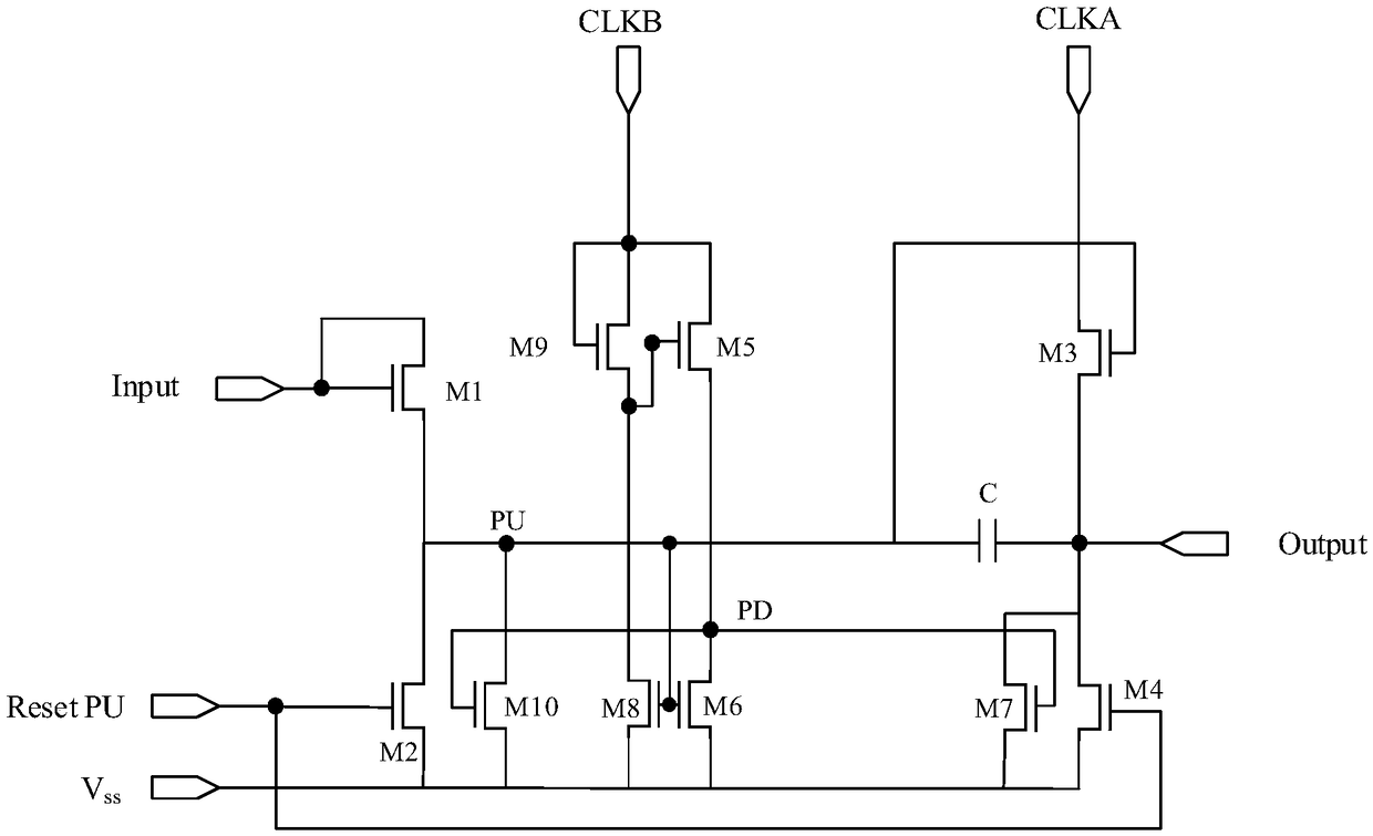
[0040] As mentioned in the background technology, in the traditional shift register circuit, the control terminals of the thin film transistor devices that control the signal input work at different temperatures, which will cause the threshold voltage drift of the thin film transistor, so that the shift register circuit can be displayed on the panel for a long time. The stability becomes worse during the process, which interferes with the output of the normal scanning signal. The related art discloses a shift register circuit, such as figure 1 As shown, the application environment of the shift register circuit is different, the actual working temperature of the thin film transistor is not fixed, and its threshold voltage will drift with the change of temperature. In the low temperature state, the threshold voltage of the first thin film transistor M1 becomes larger, and the first thin film transistor M1 is turned on later, which will lead to insufficient charging of the capaci...


PUM


Abstract

The invention discloses a shift register circuit, an array substrate and a display device. The shift register circuit comprises an input sub-circuit and a signal output sub-circuit, wherein the inputsub-circuit comprises: a control module, an input module, a voltage dividing module. The control module is connected with an input signal end and a high level signal end, and the control module is configured to output a signal of the high level signal end to a voltage dividing node under the control of an input signal; the input end of the input module is connected to the voltage dividing node, the output end of the input module is connected to the signal output sub-circuit, and the input module is configured to output a signal of the voltage dividing node to the signal output sub-circuit under the control of the control module; and the voltage dividing module is connected to the control module and a low level signal end, and the resistance value of the voltage dividing module is negatively correlated with the temperature. The signal output sub-circuit is connected to the output end of the input module, and is configured to output a gate scan signal to the output signal end under the control of the input module. The shift register circuit can improve the threshold voltage drift of the thin film transistor and improve the display stability of the display device at different temperatures.

Description

technical field [0001] The present invention relates to the field of display technology, in particular to a shift register circuit, an array substrate and a display device. Background technique [0002] TFT-LCD (Thin Film Transistor Liquid Crystal Display, Thin Film Transistor Liquid Crystal Display) includes a pixel matrix. During the display process, a gate scan signal is output through a gate drive circuit, and each pixel is scanned row by row. The gate drive circuit is used to generate the gate scanning signal of the pixel. GOA (Gate Driver on Array, array substrate row drive) is a technology that integrates the gate drive circuit on the TFT (Thin Film Transistor, thin film transistor) substrate. Each GOA unit serves as a shift register to sequentially transmit the gate scanning signal to the next GOA unit, and turn on the thin film transistor switches of the pixels row by row to complete the input of the gate scanning signal of the pixel. [0003] Since the working env...

Claims


Application Information

Patent Timeline
Patent Type & Authority Applications(China)
IPC IPC(8): G09G3/36G11C19/28
CPCG09G3/3696G11C19/28G09G2310/0286G09G2300/0408G09G2320/041G09G3/3677G09G3/3266G09G2310/0267G09G3/32G09G2310/061
Inventor 陈凯陈沫鲁思颖李方庆董文波
Owner BOE TECH GRP CO LTD
Why Eureka
Try Eureka