

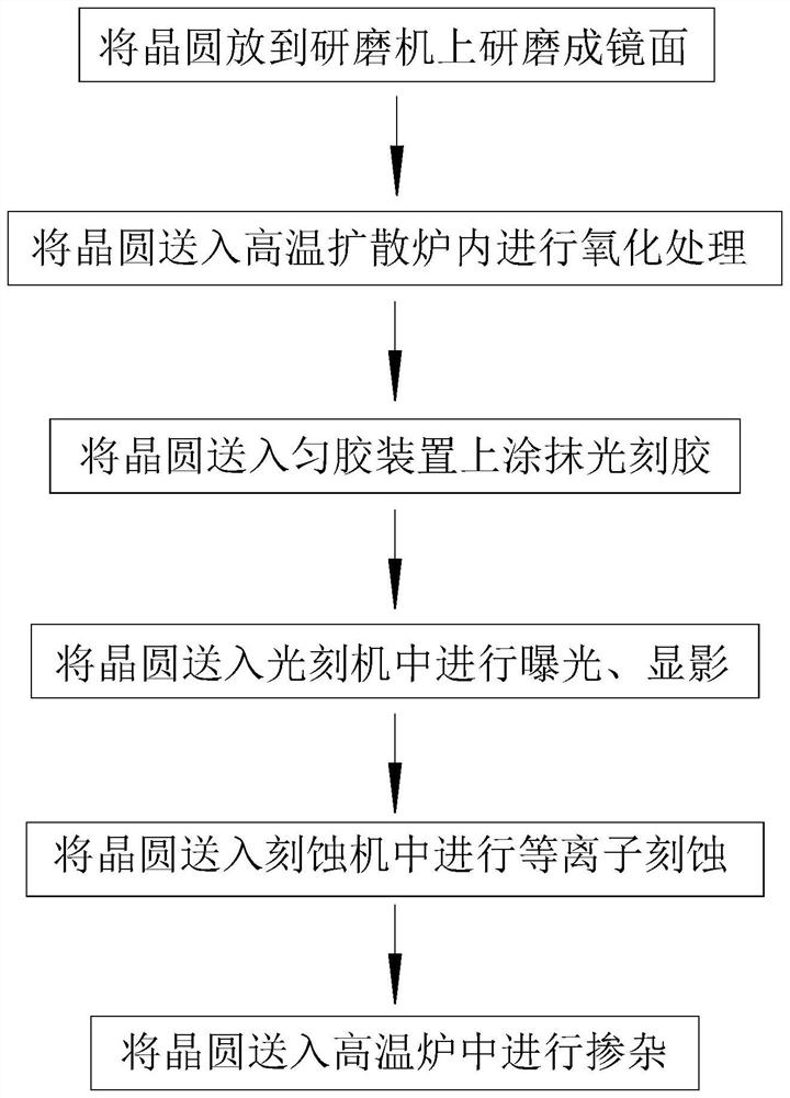
A semiconductor chip production process
A production process and semiconductor technology, applied in the fields of semiconductor/solid-state device manufacturing, electrical components, circuits, etc., can solve the problems affecting the uniformity of the glue layer, generate vibration, and cannot guarantee a smooth surface 100%, and achieve stable glue Effect
- Summary
- Abstract
- Description
- Claims
- Application Information
AI Technical Summary
Problems solved by technology
Method used
Image

Examples
Embodiment approach
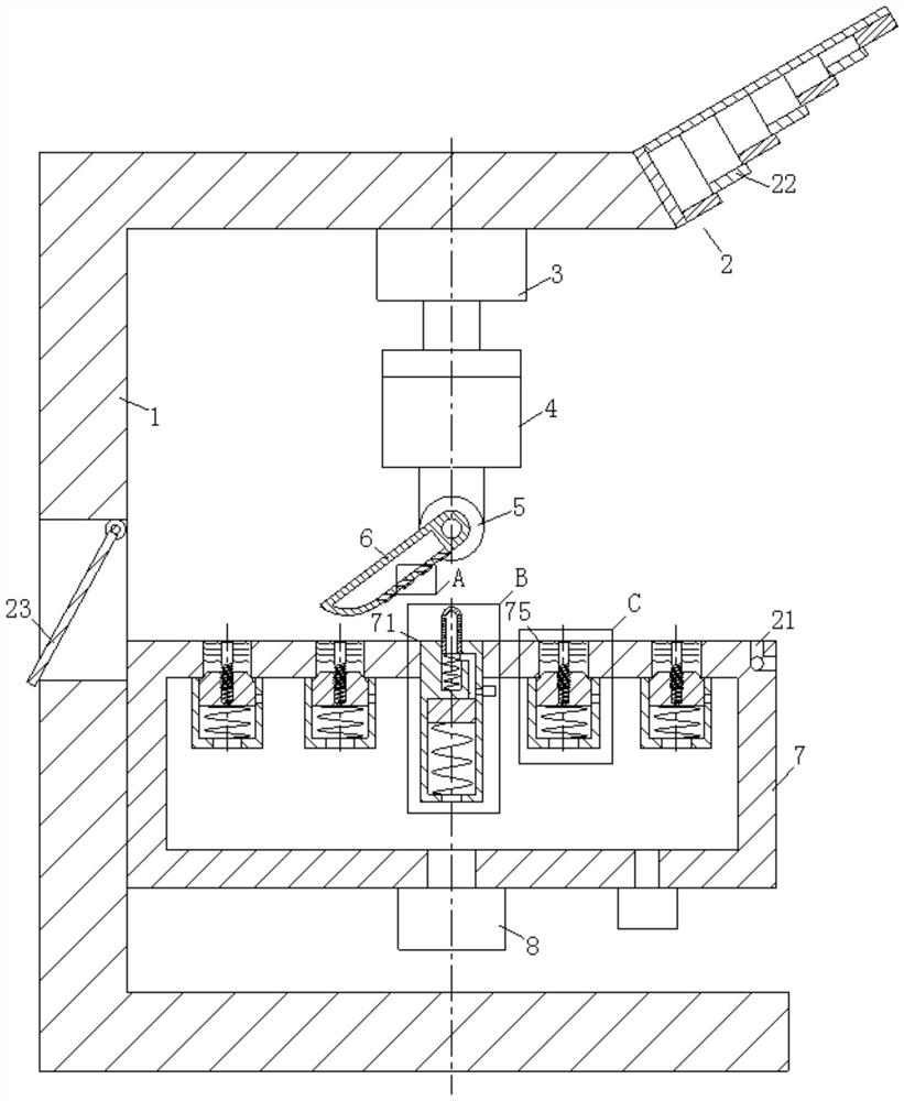
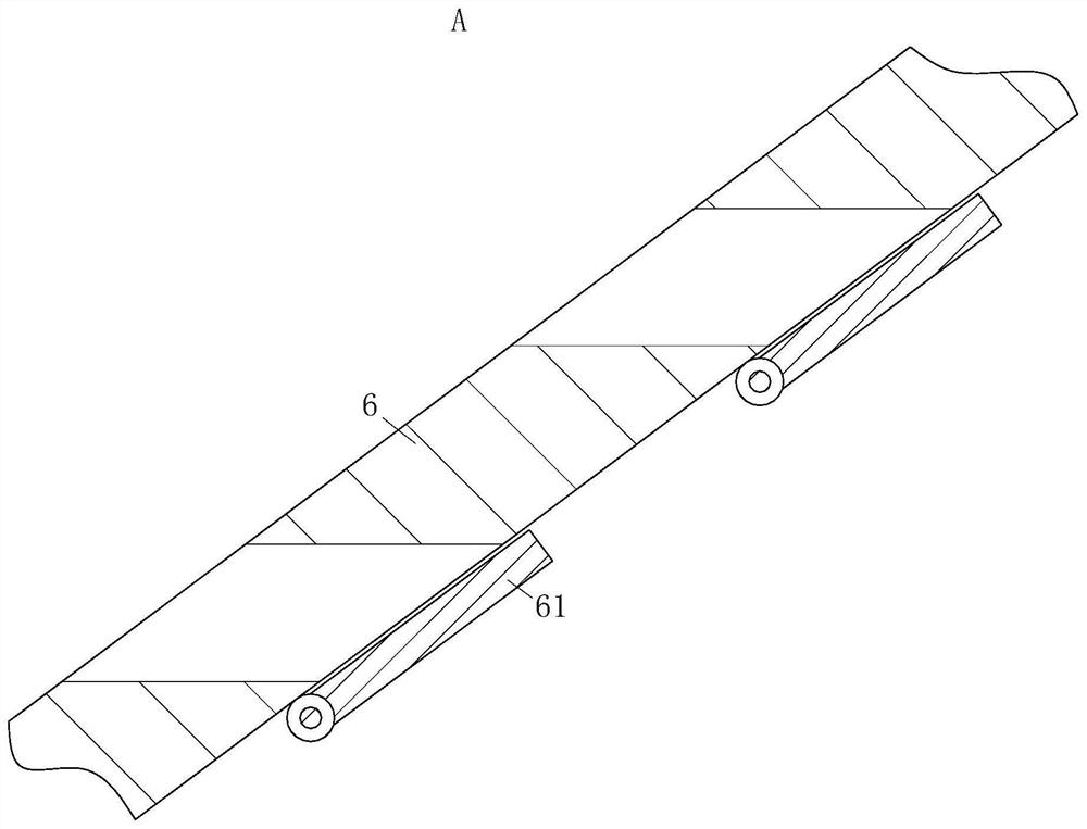
[0040] As an embodiment of the present invention, the dust blocking module 2 includes an air blowing groove 21, a pneumatic telescopic plate 22, and a dust shield 23. The air blowing groove 21 is arranged on the edge of the top plate of the workbench 7, and The air blowing groove 21 is not provided at the edge; the pneumatic expansion plate 22 is fixedly connected to the suspended side wall of the support plate 1; the pneumatic expansion plate 22 is a multi-section ejection plate, and the pneumatic expansion plate 22 is inclined upward; A rectangular hole is arranged on the vertical plate of the plate 1 near the workbench 7, and a dust shield 23 is hinged in the rectangular hole; the dust shield 23 is used to remove dust blown from the glued surface to the vertical plate of the support plate 1; the air blowing groove 21 The high-pressure compressed air is introduced to form a closed space composed of airflow above the workbench 7 to prevent dust from entering during the process...
PUM
 Abstract
Description
Claims
Application Information