
Current detection error compensation method and circuit in a voltage drop type power level circuit

A power stage circuit, current detection technology, applied in the direction of output power conversion devices, electrical components, etc., can solve the problem of inaccurate detection, and achieve the effect of accurate current excessive signal

Pending Publication Date: 2018-11-06
SICHUAN ENERGY INTERNET RES INST TSINGHUA UNIV
View PDF0 Cites 2 Cited by
  • Summary
  • Abstract
  • Description
  • Claims
  • Application Information

AI Technical Summary

Problems solved by technology

[0007] Because of the presence of parasitic inductance, this detection will become inaccurate

Method used


Image

  • Current detection error compensation method and circuit in a voltage drop type power level circuit

Examples


Embodiment approach

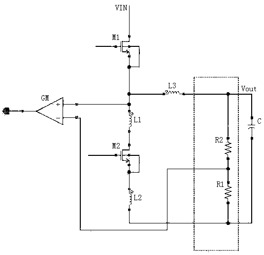
[0025] As an embodiment of the present invention, the offset voltage is the output regulation voltage of the step-down power stage circuit; after the output voltage of the step-down power stage circuit is detected and proportionally adjusted, it is fed back to the current sampling as a feedback signal The module; the proportional adjustment adjusts the sampled output voltage as an input signal to compensate and cancel the interference signal caused by the parasitic inductance on the power MOS device.

[0026] The offset is partial offset or full offset.

[0027] As an embodiment of the present invention, the ratio of the sampled output voltage is adjusted to be the ratio of the parasitic inductance to the sum of the inductances; the parasitic inductance is the sum of the parasitic inductances of the high-side and low-side MOS transistors; the sum of the inductances is high The sum of the parasitic inductance of the side MOS tube, the parasitic inductance of the low side MOS tu...


PUM


Abstract

The invention provides a current detection error compensation method and circuit in a voltage drop type power level circuit, which samples and offsets a voltage and is fed back to a current sampling module as a feedback signal. The cancellation voltage is used as an input signal to compensate and cancel the interference signal caused by the parasitic inductance on the power MOS device. The cancellation voltage is fed back to the current sampling module as the feedback signal, which can be used as the input signal compensation to offset the interference caused by the parasitic inductance of thepower level circuit, so as to obtain more accurate current zero-crossing detection signals and excessive current signals.

Description

technical field [0001] The invention relates to a current detection error compensation method and circuit in a voltage-drop type power stage circuit, and relates to the field of electronic circuits. Background technique [0002] Currently, power MOS devices are commonly used in high-current converters. These discrete MOS devices are more cost-effective than integrated devices. [0003] The larger the output current, the lower the impedance of the required MOS device. In high current applications, on-resistance below 1mOhm is common. [0004] In order to have better control over the circuit system, comprehensive protection is provided. The current on the power MOS device needs to be monitored. The current information of the power transistor can be obtained by monitoring the drain-source voltage of the turned-on power MOS device. [0005] However, since the resistance of the power tube is relatively small, the magnitude of the voltage signal obtained by the drain-source c...

Claims


Application Information

Patent Timeline
IPC IPC(8): H02M1/00
CPCH02M1/00H02M1/0009Y02B70/10
Inventor 李伊珂
Owner SICHUAN ENERGY INTERNET RES INST TSINGHUA UNIV
Learn More