Connector used for stack PCB

A connector, stacking technology, applied in the direction of connection, two-part connection device, and components of the connection device, can solve the problems of poor PCB communication, high welding process requirements, large host space, etc., to avoid direct welding, reduce Maintenance difficulty and the effect of reducing requirements

Pending Publication Date: 2018-11-09
SUNWAY COMM BEIJING
View PDF0 Cites 0 Cited by
  • Summary
  • Abstract
  • Description
  • Claims
  • Application Information

AI Technical Summary

Problems solved by technology

[0002] Existing PCB boards take up a lot of space in the host. Although the space utilization of the host can be greatly improved by stacking PCBs, the stacking between the existing PCBs is soldered together with solder paste, because the distance between the pads is less than 1mm. The welding process requires high requirements, and it is easy to have bad phenomena such as welding deviation, short circuit or open circuit, which will cause poor communication between PCBs
At the same time, in the case of stacking two PCBs, since the two PCBs have been welded to death, the upgrade can only be realized by replacing the two PCBs at the same time, and the product cannot be upgraded by replacing a single PCB.

Method used


Image

  • Connector used for stack PCB
  • Connector used for stack PCB
  • Connector used for stack PCB

Examples


Embodiment 1

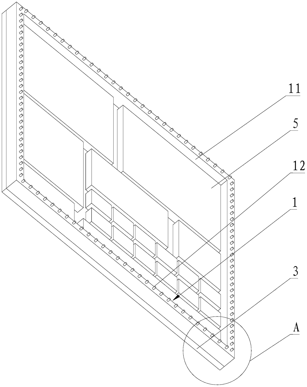
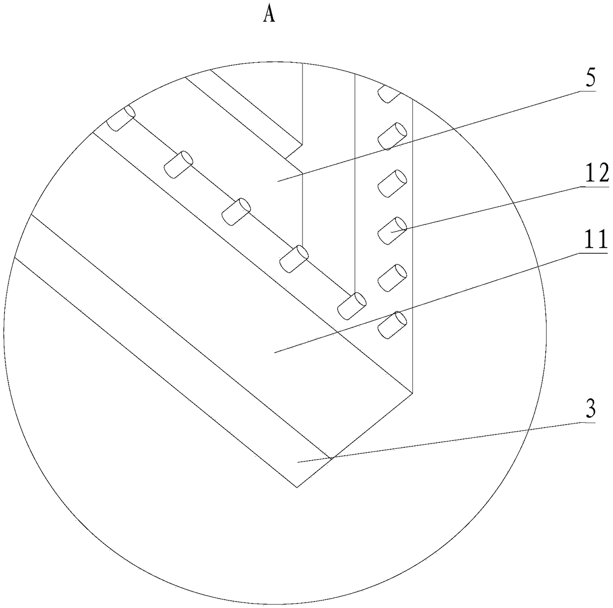
[0038] Please refer to Figure 1-5 , Embodiment 1 of the present invention is:

[0039] A connector for a stacked PCB, comprising a connector male 1 and a connector female 2, the side of the connector male 1 away from the connector female 2 is set as a male soldering surface, the connector The side of the female head 2 away from the connector male head 1 is set as the female head welding surface;

[0040] The connector male 1 includes a male housing 11, and a conductive insert 12 is arranged inside the male housing 11; one end of the conductive insert 12 extends away from the male housing 11 and extends out of the male housing 11 Outside; the other end of the conductive insert 12 is flush with the soldering surface of the male head, the conductive insert 12 is a "T"-shaped structure, and the end of the conductive insert 12 of the "T"-shaped structure with a smaller radius extends to the connection outside of male header 1.

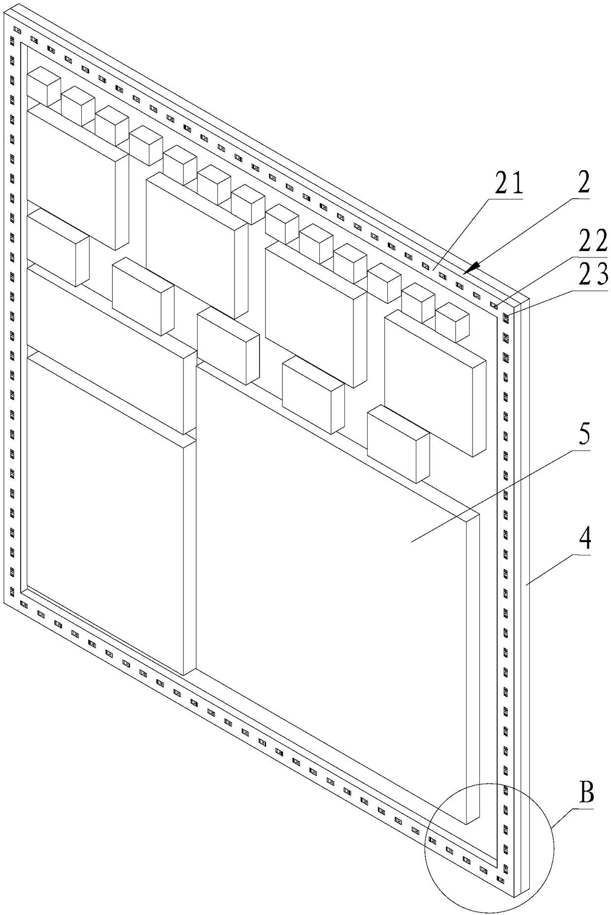
[0041] The connector female head 2 includes a fem...


PUM


Abstract

The invention provides a connector used for a stack PCB. The connector comprises a connector male head and a connector female head. The connector male head comprises a male head shell which is internally provided with a conductive plug-in. One end of the conductive plug-in extends towards the direction away from the male head shell and stretches out of the male head shell. The connector female head comprises a female head shell which is provided with jacks. The conductive plug-in is arranged in the jacks so that the connector male head and the connector female head are enabled to be electrically conducted. The connector male head and the connector female head are plugged to form a whole connector. Physical structural connection and electric signal transmission of two PCBs can be realized through the connector. Direct welding of the two PCBs can be avoided so that the requirement of the welding process can be greatly reduced and the possible risk appearing in welding can be reduced. Theconnector male head and the connector female head are conveniently detached so that maintenance in the production process can be facilitated, and the later maintenance difficulty of the client side can also be reduced. Upgrading and updating of the product can be flexibly realized.

Description

technical field [0001] The invention relates to the technical field of PCB boards, in particular to a connector for stacked PCBs. Background technique [0002] Existing PCB boards take up a lot of space in the host. Although the space utilization of the host can be greatly improved by stacking PCBs, the stacking between the existing PCBs is soldered together with solder paste, because the distance between the pads is less than 1mm. The welding process requires high requirements, and it is easy to have bad phenomena such as welding deviation, short circuit or open circuit, which will cause poor communication between PCBs. At the same time, in the case of stacking two PCBs, since the two PCBs have been welded to death, the upgrade can only be realized by replacing the two PCBs at the same time, and the product upgrade cannot be realized by replacing a single PCB. Contents of the invention [0003] The technical problem to be solved by the present invention is to provide a c...

Claims


Application Information

Patent Timeline
Patent Type & Authority Applications(China)
IPC IPC(8): H01R12/71H01R13/04H01R13/187H01R13/46H01R24/00
CPCH01R12/716H01R13/04H01R13/187H01R13/46H01R24/00
Inventor 菅永召岳向成葛立良
Owner SUNWAY COMM BEIJING
Why Eureka
Try Eureka