
Imaging system and electronic device

An imaging system and image-side technology, applied in optical components, optics, instruments, etc., can solve the problems of large imaging system size and difficulty in obtaining miniaturized imaging systems, achieve good resolution, meet high-resolution requirements, improve The effect of image quality

Pending Publication Date: 2018-11-13
JIANGXI JINGCHAO OPTICAL CO LTD
View PDF0 Cites 7 Cited by
  • Summary
  • Abstract
  • Description
  • Claims
  • Application Information

AI Technical Summary

Problems solved by technology

However, in order to correct aberrations and increase the resolution, it is usually necessary to increase the number of lenses of the imaging system, resulting in an increase in the size of the imaging system, making it difficult to obtain a miniaturized imaging system

Method used


Image

  • Imaging system and electronic device
  • Imaging system and electronic device
  • Imaging system and electronic device

Examples


no. 1 approach

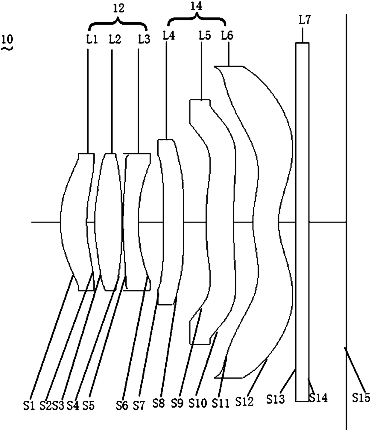
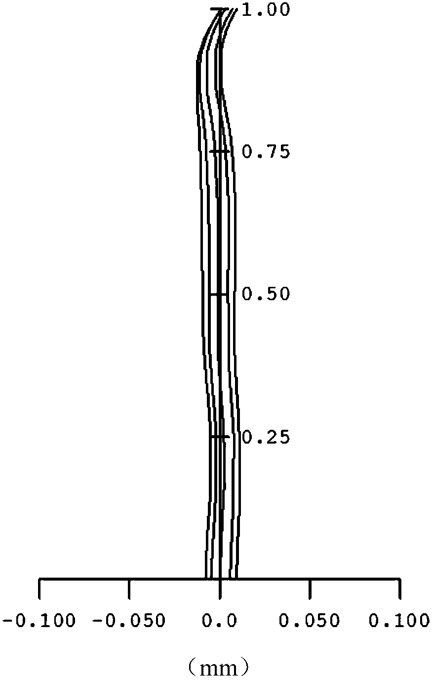
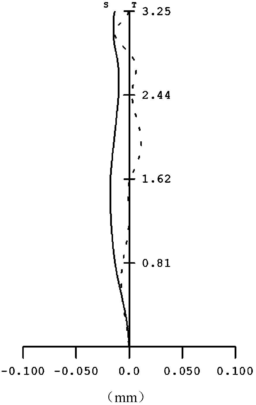
[0119] see Figure 1 to Figure 4 , the imaging system 10 satisfies the conditions of the following table:

[0120] Table 1

[0121]

[0122]

[0123] In Table 1, EFL is the effective focal length of the imaging system 10 , FNO is the focal ratio of the imaging system 10 , and FOV is the field of view of the imaging system 10 .

[0124] Table 2

[0125] Face number

[0126] The TTL of the first embodiment is 4.65, which satisfies the miniaturization requirement.

no. 2 approach

[0128] see Figure 5 to Figure 8 , the imaging system 10 satisfies the conditions of the following table:

[0129] table 3

[0130]

[0131]

[0132] In Table 3, EFL is the effective focal length of the imaging system 10 , FNO is the focal ratio of the imaging system 10 , and FOV is the field of view of the imaging system 10 .

[0133] Table 4

[0134] Face number

[0135] The TTL of the second embodiment is 4.75, meeting the miniaturization requirement.

no. 3 approach

[0137] see Figure 9 to Figure 12 , the imaging system 10 satisfies the conditions of the following table:

[0138] table 5

[0139]

[0140] In Table 5, EFL is the effective focal length of the imaging system 10 , FNO is the focal ratio of the imaging system 10 , and FOV is the field of view of the imaging system 10 .

[0141] Table 6

[0142]

[0143]

[0144] The TTL of the third embodiment is 4.75, meeting the miniaturization requirement.


PUM


Abstract

The invention discloses an imaging system and an electronic device. The imaging system includes a first lens with positive refractive power, a second lens with refractive power, a third lens with refractive power, a fourth lens with refractive power, a fifth lens with positive refractive power and a sixth lens with negative refractive power, in order from the object side to the image side of an optical axis, wherein the object side surface of the first lens is a convex surface; the object side surface of the fifth lens is a concave surface at the circumference; the image side surface of the fifth lens is a convex surface; the image side surface of the sixth lens is a concave surface at the optical axis; the image side surface of the sixth lens is a convex surface at the circumference; andat least one of the object side surface and the image side surface of the sixth lens includes at least one inflexion point. For the imaging system and the electronic device, through the above-mentioned reasonable lens configuration of six lenses, the imaging system not only has a good resolution to meet the high resolution requirement, but also can reduce the height of the imaging system to meet the demand for miniaturization.

Description

technical field [0001] The invention relates to optical imaging technology, in particular to an imaging system and an electronic device. Background technique [0002] With the development of semiconductor technology, the pixels of the photosensitive element are getting higher and higher, so the requirement for the resolution of the imaging system that cooperates with the photosensitive element is also getting higher and higher. However, in order to correct aberrations and increase resolution, it is usually necessary to increase the number of lenses of the imaging system, resulting in a larger size of the imaging system, making it difficult to obtain a miniaturized imaging system. Contents of the invention [0003] Embodiments of the present invention provide an imaging system and an electronic device. [0004] The imaging system according to the embodiment of the present invention includes a first lens with positive refractive power, a second lens with refractive power, a...

Claims


Application Information

Patent Timeline
Patent Type & Authority Applications(China)
IPC IPC(8): G02B13/00G02B13/18
CPCG02B13/0045G02B13/18
Inventor 邹海荣俞炳泽兰宾利
Owner JIANGXI JINGCHAO OPTICAL CO LTD
Learn More