Array substrate, manufacturing method thereof and display panel

A technology of array substrate and substrate substrate, applied in semiconductor/solid-state device manufacturing, optics, instruments, etc., can solve problems such as electrostatic breakdown of the second capacitor, and achieve the effect of avoiding electrostatic breakdown

Active Publication Date: 2018-11-23
BOE TECH GRP CO LTD +1
View PDF6 Cites 2 Cited by
  • Summary
  • Abstract
  • Description
  • Claims
  • Application Information

AI Technical Summary

Problems solved by technology

[0005] The present application provides an array substrate, a manufacturing method thereof, and a display panel, which can solve the problem in the prior art that more electrostatic charges are accumulated in the second capacitor, which easily leads to electrostatic breakdown of the second capacitor. The technical solution as follows:

Method used


Image

  • Array substrate, manufacturing method thereof and display panel
  • Array substrate, manufacturing method thereof and display panel
  • Array substrate, manufacturing method thereof and display panel

Examples


Embodiment Construction

[0045] In order to make the purpose, technical solution and advantages of the present application clearer, the implementation manners of the present application will be further described in detail below in conjunction with the accompanying drawings.

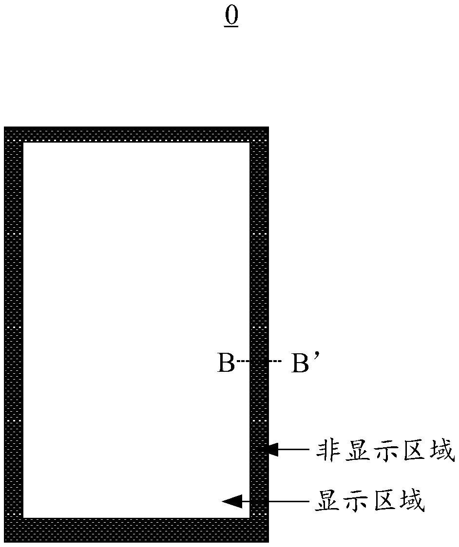
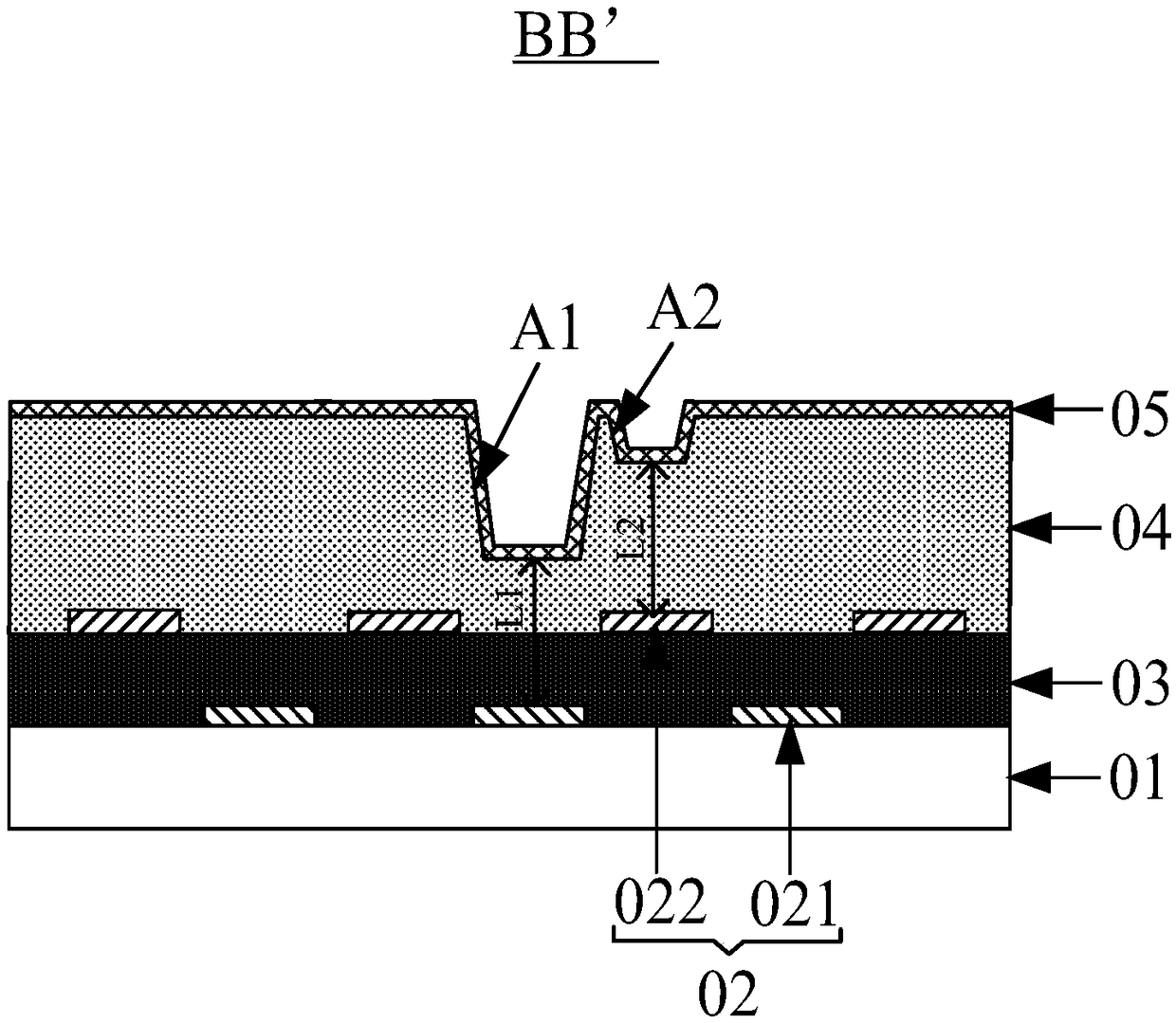
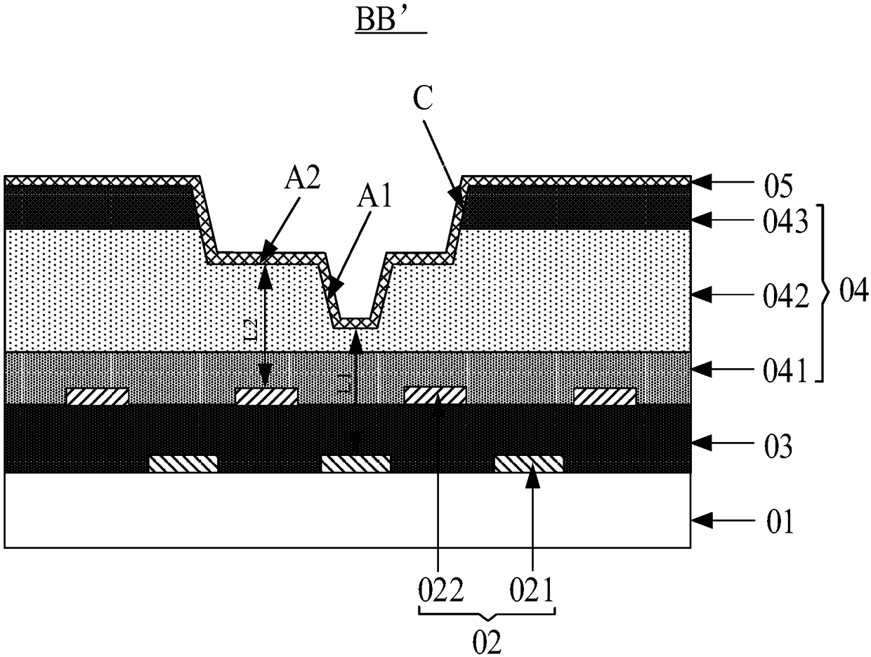
[0046] figure 1 An array substrate provided for an embodiment of the present invention, such as figure 1 As shown, the array substrate 0 can be divided into a display area and a non-display area. figure 2 A kind of provided for the embodiment of the present invention figure 1 Schematic diagram of section BB' of the non-display area of ​​the array substrate.

[0047] Depend on figure 2 It can be seen that the array substrate 0 may include a base substrate 01 . A conductive structure 02 is disposed on the base substrate 01 , and the conductive structure 02 includes superimposed gate lines 021 and data lines 022 . An insulating structure 04 is disposed on the conductive structure 02 , and a common electrode layer 05 is formed...


PUM


Abstract

The invention discloses an array substrate, a manufacturing method thereof and a display panel, and belongs to the technical field of displaying. The array substrate comprises a substrate body; the substrate body is provided with a conduction structure, and the conduction structure comprises overlapped grid lines and data lines; the conduction structure is provided with an insulating structure; apublic electrode layer is formed on the insulating structure; first sunken structures right facing the grid lines and second sunken structures right facing the data lines are arranged at the portion,in a non-display area of the substrate body, in the insulating structure, openings of the first sunken structures and the second sunken structures are all away from the substrate body, and the distance between the bottom faces of the first sunken structures and the grid lines is equal to the distance between the bottom faces of the second sunken structures and the data lines. By means of the arraysubstrate, the manufacturing method thereof and the display panel, the problem that a second capacitor is easily subjected to electrostatic breakdown when there are many electrostatic charges accumulated in the second capacitor is solved, and the manufacturing method of the array substrate and the display panel are used for the array substrate.

Description

technical field [0001] The present application relates to the field of display technology, in particular to an array substrate, a manufacturing method thereof, and a display panel. Background technique [0002] The liquid crystal display panel mainly includes an array substrate and a color filter substrate disposed opposite to each other, and a liquid crystal layer arranged between the color filter substrate and the array substrate. [0003] The array substrate usually includes: a base substrate, and a gate line, a gate insulating layer, a data line, a data insulating layer, a flat layer, a passivation layer, and a common electrode layer arranged sequentially on the base substrate, and the gate line and the common electrode layer A first capacitor is formed between the data line and the common electrode, and a second capacitor is formed between the data line and the common electrode. Since the distance between the gate line and the common electrode layer is greater than the...

Claims


Application Information

Patent Timeline
Patent Type & Authority Applications(China)
IPC IPC(8): G02F1/1362H01L27/12H01L21/77
CPCG02F1/136204G02F2202/22G02F1/136295H01L27/124H01L27/1259
Inventor 曹诚英
Owner BOE TECH GRP CO LTD
Why Eureka
Try Eureka