Biometric chip module packaging device and packaging method therefor

A chip module and packaging equipment technology, applied in the field of biometric chip module packaging equipment and its packaging, can solve the problems of reducing production line utilization rate, increasing packaging operation time, and spending a lot of time, so as to improve operation efficiency and increase utilization The effect of high efficiency and smooth operation process

Inactive Publication Date: 2018-11-23
D TEK TECHNOLOGY CO LTD
View PDF5 Cites 0 Cited by
  • Summary
  • Abstract
  • Description
  • Claims
  • Application Information

AI Technical Summary

Problems solved by technology

[0004] The disadvantage of the above-mentioned prior art is that the traditional packaging equipment uses three image recognition units and two pick-and-place machines to perform three visual recognition processes to confirm the precise position of the above-mentioned materials, and then perform two visual recognition processes based on the above-mentioned visual recognition processing data. The second material is picked up, and after all the parts are placed, the packaging operation is finally carried out
It takes a lot of time to move three image recognition units and two pick-and-place machines, and perform three visual recognition processes
[0005] Therefore, if the traditional packaging equipment is faced with a large number of packaging operations, it will inevitably lead to a significant increase in the packaging operation time, reduce the utilization rate of the production line, and then affect the follow-up operation capacity

Method used


Image

  • Biometric chip module packaging device and packaging method therefor
  • Biometric chip module packaging device and packaging method therefor
  • Biometric chip module packaging device and packaging method therefor

Examples


Embodiment Construction

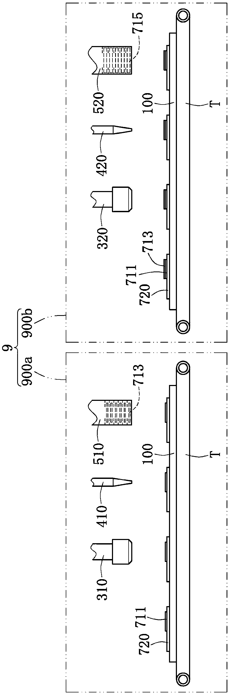
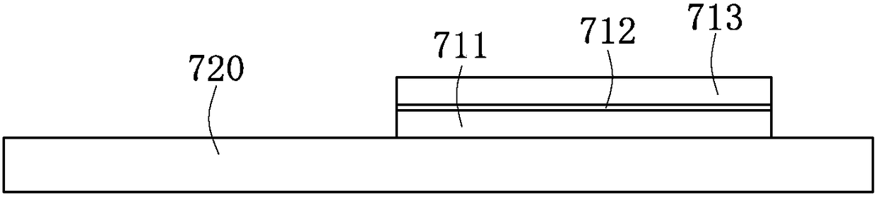
[0019] figure 1 It is a schematic diagram of an embodiment of the biometric chip module packaging device of the present invention. The biometric chip module packaging equipment 9 provides a first operation station 900a and a second operation station 900b. The first operating station 900a has a flat carrier plate 100 for placing a plurality of biometric chip modules to be assembled. The carrier board 100 is transported to the first operation station 900a by a conveyor belt T. Referring to FIG. The first operating station 900 a provides a first image recognition unit 310 located above the carrier board 100 . The first image recognition unit 310 can move in multiple axes, so that the first image recognition unit 310 can be moved to any corner of the carrier board 100 to sequentially acquire multiple circuit boards 720 and biometric chips on the carrier board 100 Step 711 forms an image of the biometric chip module to be assembled, and transmits the acquired image to a computin...


PUM


Abstract

The invention relates to a biometric chip module packaging device and a packaging method therefor. The biometric chip module packaging device includes: a first operation station, used for accommodating a carrier plate. At least one circuit board and a biometric chip are placed on the carrier plate. The first operation station includes a first image recognition unit, a first gluing device and a first cartridge-type material tube. The first image recognition unit is used for recognizing the locations of the circuit board and the biometric chip on the carrier plate. The first gluing device receives information of the locations of the circuit board and the biometric chip from the first image recognition unit, and coats the biometric chip with conductive glue or places a conductive glue plate on the biometric chip. The first cartridge-type material tube accommodates at least one protection plate. The first cartridge-type material tube receives the information of the locations of the circuitboard and the biometric chip from the first image recognition unit, and places the protection plate on the top surface of the biometric chip to perform assembling. The biometric chip module packagingdevice further includes a second operation station for placing a placement frame on the top surface of the protection plate.

Description

technical field [0001] The invention relates to a biometric identification chip module packaging device and a packaging method thereof, in particular to a biometric identification chip module packaging device with a magazine-type material tube and a packaging method thereof. Background technique [0002] Biometric (Biometric) refers to the use of each person's unique physiological or behavioral characteristics, such as human fingerprints, faces, voices or irises, to identify users. Taking fingerprint identification as an example, the fingerprint identification chip package structure can be installed in various electronic products, such as smart phones, mobile phones, tablet computers, notebook computers and personal digital assistants (PDAs), etc., to identify users' fingerprints . Existing fingerprint recognition chip packages can be roughly classified into packages using a flexible circuit board or a rigid circuit board as a carrier. The fingerprint identification chip p...

Claims


Application Information

Patent Timeline
Patent Type & Authority Applications(China)
IPC IPC(8): H01L21/56H01L23/31H01L23/488
CPCH01L21/561H01L23/3107H01L23/488H01L2224/83
Inventor 王振华高立群陈志辉李能旺巫沛学
Owner D TEK TECHNOLOGY CO LTD
Why Eureka
Try Eureka