Infrared semiconductor avalanche detector and its preparation method

A semiconductor and detector technology, applied in the field of infrared semiconductor avalanche detectors and their preparation, can solve the problems of difficult material growth, difficult to realize detection, and limit the application range of detectors, achieve low excess noise, and improve ionization coefficient ratio. , the effect of high gain

Active Publication Date: 2020-05-12
TSINGHUA UNIV
View PDF6 Cites 0 Cited by
  • Summary
  • Abstract
  • Description
  • Claims
  • Application Information

AI Technical Summary

Problems solved by technology

However, since GaN and AlN are wide-bandgap semiconductors, the absorption spectrum is in the ultraviolet region, which limits the application range of the detector.
And because the lattice constants of GaN and AlN materials are quite different from the lattice constants of narrow bandgap semiconductors suitable for infrared absorption, the material growth is extremely difficult, so it is difficult to realize the detection of infrared light by using GaN and AlN materials as multiplication layers

Method used


Image

  • Infrared semiconductor avalanche detector and its preparation method
  • Infrared semiconductor avalanche detector and its preparation method
  • Infrared semiconductor avalanche detector and its preparation method

Examples


Embodiment Construction

[0041] In order to make the purpose, technical solutions and advantages of the present disclosure clearer, the present disclosure will be further described in detail below in conjunction with specific embodiments and with reference to the accompanying drawings.

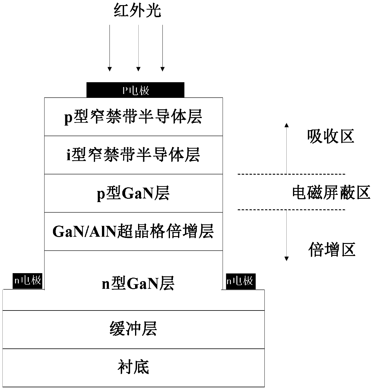
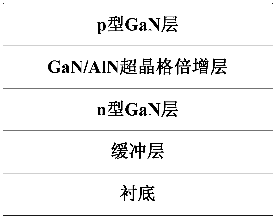
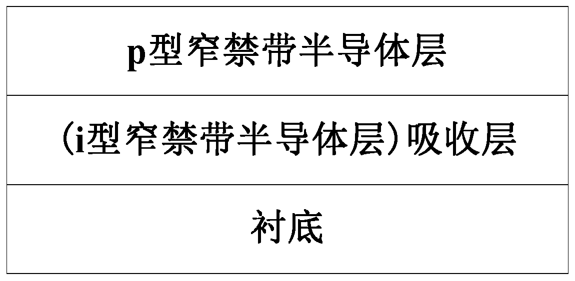
[0042] To meet the demand for high-gain linear avalanche detectors in the infrared band, the present disclosure provides an infrared semiconductor avalanche detector with a narrow bandgap semiconductor as the absorption region and a GaN / AlN superlattice material as the multiplication region and its preparation method. In this disclosure, the i-region of the traditional p-i-n structure and the thin p-layer with high doping concentration are separated to form a separate absorption layer and a multiplication layer. The electric field is mainly distributed in the GaN / AlN superlattice multiplication layer, and the infrared light is blocked by a narrow band gap. The semiconductor absorption layer absorbs and transforms into ...


PUM

PropertyMeasurementUnit
thicknessaaaaaaaaaa
thicknessaaaaaaaaaa
thicknessaaaaaaaaaa

Abstract

The invention provides an infrared semiconductor avalanche detector and a preparation method thereof. The infrared semiconductor avalanche detector comprises a GaN / AlN superlattice multiplication structure and a narrow bandgap semiconductor absorption structure on the GaN / AlN superlattice multiplication structure, wherein the GaN / AlN superlattice multiplication structure and the narrow bandgap semiconductor absorption structure are in bonding connection. According to the infrared semiconductor avalanche detector and the preparation method, the ionization coefficient ratio of electron holes isimproved, the unipolar ionization of electrons is achieved, the excess noise is reduced, and a high gain is provided.

Description

technical field [0001] The present disclosure relates to the technical field of semiconductor detection, and in particular to an infrared semiconductor avalanche detector based on a GaN / AlN periodic structure multiplication layer and a preparation method thereof. Background technique [0002] Any substance above absolute zero (-273.15°C) can generate infrared light, which contains rich information about the substance. Therefore, infrared detection is one of the main means for human beings to obtain information. It converts invisible infrared radiation into measurable electrical signals, enabling people to obtain more abundant information about the objective world. The unique spectral characteristics of the infrared band make it have important applications in thermal imaging, infrared remote sensing, military defense, medical detection, and optical fiber communication, and optoelectronic detection devices for the infrared band are the key technologies to realize these applica...

Claims


Application Information

Patent Timeline
Patent Type & Authority Patents(China)
IPC IPC(8): H01L31/0352H01L31/107H01L31/18
CPCH01L31/035236H01L31/1075H01L31/184H01L31/1856Y02P70/50
Inventor 汪莱刘洋吴星曌郝智彪罗毅
Owner TSINGHUA UNIV
Why Eureka
Try Eureka