Unlock instant, AI-driven research and patent intelligence for your innovation.

Logic level conversion circuit and integrated circuit

A technology for converting circuits and logic levels, applied in the direction of logic circuit connection/interface layout, etc., can solve the problems of IO port damage, increase of bit error rate, communication failure, etc.

Inactive Publication Date: 2018-11-30
比飞力(深圳)科技有限公司
View PDF16 Cites 0 Cited by
  • Summary
  • Abstract
  • Description
  • Claims
  • Application Information

AI Technical Summary

Problems solved by technology

[0005] When the lower-level chip U 1 To the upper chip U 2 When the transmitted level signal is high level, the upper chip U 2 The high-level voltage of the received level signal is VIO-Vcore. When the high-level voltage of VIO-Vcore is lower than the normal high-level VIO voltage, the bit error rate will be greatly increased, resulting in communication failure.
[0006] Assuming Vcore=0.4V, VIO=1.8V, the voltage difference of the same logic level between different level chips is 0.4V, that is, when the lower level chip U 1 To the upper chip U 2 The low level of the transmitted level signal is 0V, and the upper chip U 2 The low-level voltage of the received level signal is -0.4V, which will cause damage to the IO port; when the lower-level chip U 1 To the upper chip U 2 When the high level of the transmitted level signal is 1.8V, the upper chip U 2 The high level of the received level signal is 1.4V, if it is lower than 1.8V, the bit error rate will be greatly increased, resulting in communication failure

Method used


Image

  • Logic level conversion circuit and integrated circuit
  • Logic level conversion circuit and integrated circuit
  • Logic level conversion circuit and integrated circuit

Examples


Embodiment Construction

[0021] In order to make the above objects, features and advantages of the present invention more comprehensible, the present invention will be further described in detail below in conjunction with the accompanying drawings and specific embodiments.

[0022] The embodiment of the present invention proposes a logic level conversion circuit, so that the voltage of the level signal transmitted by the lower-level chip can match the working voltage of the upper-level chip, and the cascaded chips can work normally.

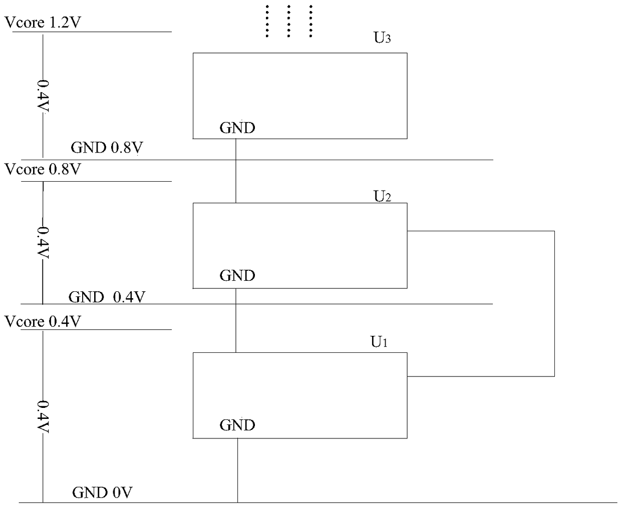
[0023] refer to figure 2 , shows a structural block diagram of an embodiment of a logic level conversion circuit of the present invention, the logic level conversion circuit of the embodiment of the present invention is applied to a cascaded chip, and the cascaded chip may include N-level chips connected in series, where N is an integer greater than 1.

[0024] In the embodiment of the present invention, the logic level conversion circuit is connected between the M-1th...


PUM


Abstract

The embodiment of the invention provides a logic level conversion circuit and an integrated circuit, applied to a cascaded chip, the cascaded chip comprises N levels of chips connected in series, theN is an integer greater than 1, the logic level conversion circuit is connected between the (M-1)th level chip in the cascaded chip and the Mth level chip in the cascaded chip, and the M is an integergreater than 1 and less than or equal to N; the logic level conversion circuit is used for converting the voltage of a level signal into a target voltage when the (M-1)th level chip transmits the level signal to the Mth level chip, and sending the level signal in which the voltage is the target voltage to the Mth level chip; and the target voltage is matched with a working voltage of the Mth level chip. By application of the logic level conversion circuit provided by the embodiment of the invention, the following problems are avoided: an IO port is damaged due to a negative pressure, and thebit error rate is increased due to lower than the normal working voltage, resulting in communication failure.

Description

technical field [0001] The invention relates to the technical field of electronic circuits, in particular to a logic level conversion circuit and an integrated circuit. Background technique [0002] With the development of electronic technology, there are more and more various electronic devices to meet people's different needs, such as electronic devices that need to use many chips for specific data processing. [0003] At present, for electronic equipment with many chips, such as special-purpose computing equipment, the chips are cascaded applications. The so-called cascaded application refers to connecting multiple circuit structures with the same or similar functions in a regular connection manner. Specifically, Chip cascading means that the negative pole of the power supply of the upper chip is connected to the positive pole of the power supply of the lower chip. At present, some schemes connect the two chips directly, and some schemes add resistors between the two chip...

Claims


Application Information

Patent Timeline
IPC IPC(8): H03K19/0175
CPCH03K19/0175
Inventor 郭斌
Owner 比飞力(深圳)科技有限公司