Touch display device and driving method thereof

A technology of a touch display device and a driving method, which is applied in the fields of instruments, computing, and electrical and digital data processing, etc., can solve problems such as poor touch control, poor display, and short circuit of signal lines.

Pending Publication Date: 2018-12-07
BOE TECH GRP CO LTD +1
View PDF4 Cites 0 Cited by
  • Summary
  • Abstract
  • Description
  • Claims
  • Application Information

AI Technical Summary

Problems solved by technology

figure 1 is a structural schematic diagram of an existing touch display substrate, which adopts a self-capacitance structure, such as figure 1 As shown, the touch display substrate 10 includes a plurality of common electrodes 11, and each common electrode 11 is connected to the drive circuit 20 through a touch signal line TXL; at the same time, the thin film transistors

Method used


Image

  • Touch display device and driving method thereof
  • Touch display device and driving method thereof
  • Touch display device and driving method thereof

Examples


Embodiment 1

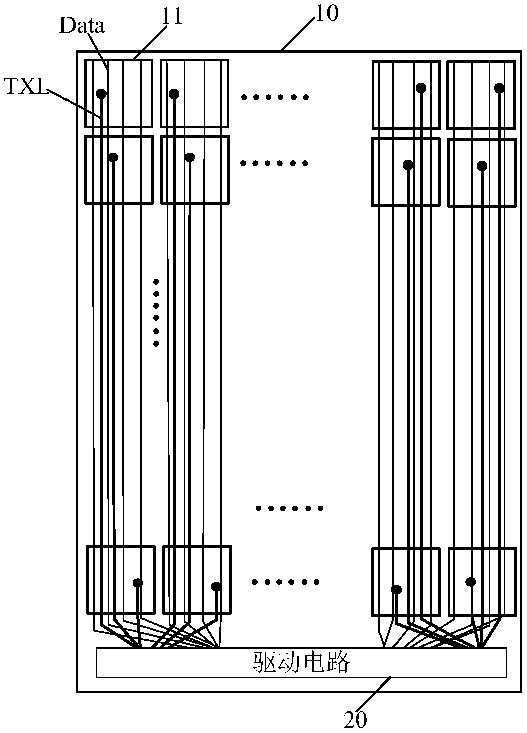
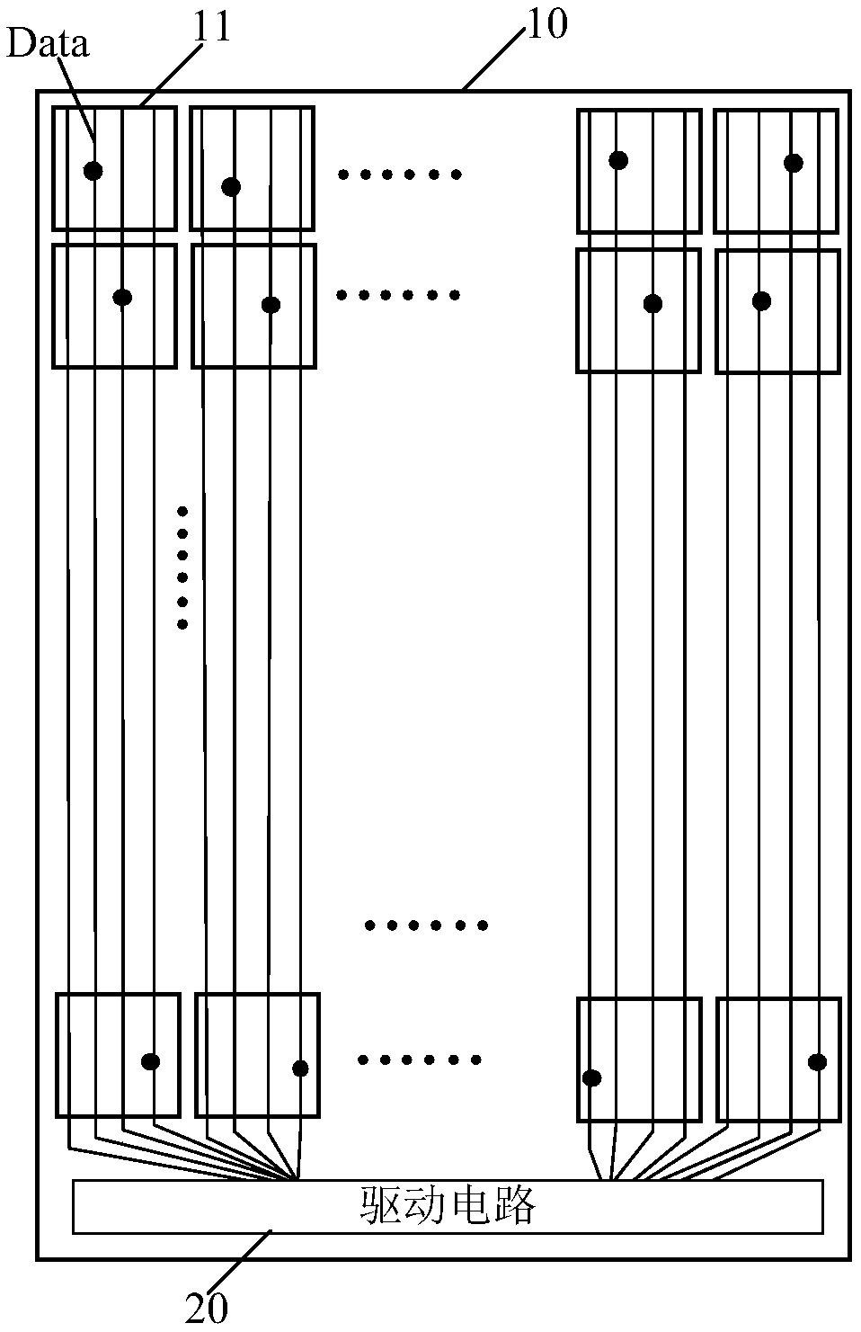
[0033] figure 2 It is a schematic diagram of the touch display device provided by Embodiment 1 of the present invention, as shown in figure 2 As shown, the touch display device includes a touch display substrate 10 and a driving circuit 20 , and the touch display substrate 10 includes a plurality of data lines Data and a plurality of common electrodes 11 . The common electrodes 11 are multiplexed as touch driving electrodes in the touch stage, and each common electrode 11 corresponds to one data line Data. The driving circuit 20 is used to provide display signals for the data lines Data in the display phase, and provide touch signals for the data lines corresponding to the common electrodes 11 in the touch phase.

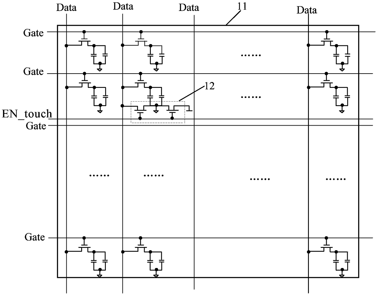
[0034] image 3 is a structural schematic diagram of the area where one of the common electrodes on the touch display substrate is located. Such as image 3 As shown, the touch display substrate 10 also includes a gate unit 12 corresponding to the common elect...

Embodiment 2

[0046] Embodiment 2 of the present invention provides a driving method of the above-mentioned touch display device, the driving method comprising:

[0047] In the display stage, the drive circuit provides display signals to each of the data lines, and the gate unit conducts the common electrode with the common signal terminal.

[0048] In a touch stage, the drive circuit provides a touch signal to the data line corresponding to the common electrode.

[0049] As mentioned above, the touch display substrate further includes a gate control line, and the gate unit includes a first transistor and a second transistor. At this time, the driving method further includes:

[0050] In the touch phase, the drive circuit provides a first control signal to the gate control line, the first control signal is used to control the first transistor to turn on, and control the second transistor to turn off .

[0051] In the display phase, the drive circuit provides a second control signal to the...


PUM


Abstract

Provided is a touch display device, which includes a touch display substrate and a driving circuit, the touch display substrate includes a plurality of data lines and a plurality of common electrodes,the common electrode is multiplexed into a touch driving electrode in a touch control stage, each common electrode corresponds to a data line, and the driving circuit is used for supplying a displaysignal to the data line in a display stage and supplying a touch signal to the data line corresponding to the common electrode in a touch control stage. The touch display substrate further comprises agating unit corresponding to the common electrode one by one, wherein the gating unit is connected with a corresponding common electrode, a data line corresponding to the common electrode and a common signal terminal, and is used for transmitting a touch signal on the data line to the common electrode in the touch control stage; and conducting the common electrode with the common signal terminalin a display stage. The invention also provides a driving method of a touch display device. The invention can reduce the phenomenon of short circuit between signal wires.

Description

technical field [0001] The present invention relates to the field of touch display, in particular to a touch display device and a driving method thereof. Background technique [0002] At present, in many touch display devices, a time-division multiplexing method is used for touch and display, that is, a common voltage signal is provided to the common electrodes in the display phase, and a touch driving signal is provided to the common electrodes in the touch phase. figure 1 is a structural schematic diagram of an existing touch display substrate, which adopts a self-capacitance structure, such as figure 1 As shown, the touch display substrate 10 includes a plurality of common electrodes 11, and each common electrode 11 is connected to the drive circuit 20 through a touch signal line TXL; at the same time, the thin film transistors in each column of pixels are connected to each other through a data line Data The driving circuits 20 are connected together, which leads to the ...

Claims


Application Information

Patent Timeline
IPC IPC(8): G06F3/041
CPCG06F3/0412G06F3/0416
Inventor 陈利峰石天雷赵小恒陈文君李文可刘白灵赵顺毕海峰王鑫包玉峰方燕
Owner BOE TECH GRP CO LTD
Why Eureka
Try Eureka