
pm-oled display substrate and manufacturing method thereof

A PM-OLED and display substrate technology, applied in the field of PM-OLED display substrate and its production, can solve the problem of single and double effect of PM-OLED display panel, so as to improve the problem of single and double effect, ensure display effect and improve product quality Effect

Active Publication Date: 2020-05-12
TRULY SEMICON
View PDF3 Cites 0 Cited by
  • Summary
  • Abstract
  • Description
  • Claims
  • Application Information

AI Technical Summary

Problems solved by technology

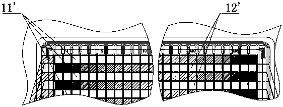
[0003] The technical problem to be solved by the present invention is to be able to effectively solve the problem of single and double effects when the PM-OLED display panel is fully lit.

Method used


Image

  • pm-oled display substrate and manufacturing method thereof
  • pm-oled display substrate and manufacturing method thereof
  • pm-oled display substrate and manufacturing method thereof

Examples


Embodiment 1

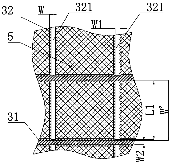
[0038] Such as Figure 2-3As shown, it represents a PM-OLED display substrate provided by the present invention. The PM-OLED display substrate includes SEG traces 1, COM traces 2, pixel insulation grids 3, isolation columns 4, and pixel units 5 arranged in an array, and also includes a set corresponding to the pixel insulation grids 3 and connected to the pixel insulation grids 3. The auxiliary electrode line 6 electrically connected to the SEG line 1, the pixel insulation grid 3 includes a SEG direction insulating strip 31 in the same direction as the SEG line 1 and a COM direction in the same direction as the COM line 2 Insulating strips 32 , the auxiliary electrode lines 6 are accommodated in the pixel insulating grid 3 , and the PM-OLED display substrate provided in this embodiment further includes a substrate 10 . In this way, by arranging the auxiliary electrode lines 6 housed in the pixel insulating grid 3 and electrically connected to the SEG lines 1, that is, in the ...

Embodiment 2

[0041] The principle of this embodiment is the same as that of the above embodiment, and the structure is similar, and the only difference is that, as Figure 4 As shown, the wiring slots opened on the pixel insulating grid 3 also include the SEG wiring slots 311 located on the SEG insulating strips 31 . That is, in this embodiment, the COM-direction insulating strip 32 on the pixel isolation grid 3 is provided with a COM-direction wiring groove 321 , and the SEG-direction insulating strip 31 is provided with a SEG-direction wiring groove 311 . In this way, the layout position of the auxiliary electrode lines 6 is effectively increased, thereby making the resistance of the auxiliary electrode lines 6 smaller, further improving the effect of reducing the resistance of the auxiliary electrode lines 6, effectively ensuring the effect of improving the single-double effect, and ensuring the display brightness. uniform. Specifically, the width W of the SEG to the wiring groove 311 ...

Embodiment 3

[0043] The principle of this embodiment is the same as that of the above embodiment, and the structure is similar, and the only difference is that, as Figure 5 As shown, the isolation column 4 in the PM-OLED display substrate provided by this embodiment is provided with an isolation column groove 41 for accommodating the auxiliary electrode line 6 . That is, in this embodiment, the pixel insulation grid 3 is provided with a COM-direction wiring groove 321 and a SEG-direction wiring groove 311 , and an isolation column groove 41 is opened on the isolation column 4 . In this way, the auxiliary electrode lines 6 accommodated in the pixel insulating grid 3 can further increase the layout position, and at the same time be accommodated in the isolation groove 41, thereby further ensuring that the resistance of the auxiliary electrode lines 6 is small, and ensuring that the auxiliary electrode lines 6 reduce resistance. In order to improve the effect of single and double effects, en...


PUM


Abstract

The invention provides a PM-OLED display substrate and a manufacturing method thereof. The PM-OLED display substrate includes SEG wiring, COM wiring, pixel insulating grids, isolation columns and pixel units arranged in an array, and the pixel insulating grid It includes a SEG-directed insulating strip in the same direction as the SEG trace and a COM-directed insulating strip in the same direction as the COM trace, and also includes a set corresponding to the pixel insulation grid and electrically connected to the SEG trace The auxiliary electrode lines are accommodated in the pixel insulating grid or covered under the pixel insulating grid. The PM-OLED display substrate provided by the present invention can effectively reduce the resistance difference between the beginning section and the end end of the SEG wiring, improve the single-double effect problem, effectively ensure the display effect, and improve product quality. The manufacturing method of the PM-OLED display substrate provided by the present invention can effectively realize the manufacturing of the PM-OLED display substrate, and can effectively improve production efficiency.

Description

technical field [0001] The invention relates to the field of display technology, in particular to a PM-OLED display substrate and a manufacturing method thereof. Background technique [0002] PM-OLED display technology is called the third-generation fantasy display technology because of its advantages such as all-solid-state active light emission, good temperature characteristics, low power consumption, fast response, bendable and foldable, and ultra-thin. Due to the gradual increase of the resistance of the SEG wiring of the existing PM-OLED display substrate, in the case of full lighting, between the start position and the end position of the SEG wiring in the light-emitting area, due to the gradual increase of the resistance, the SEG There must be a certain voltage drop between the start end and the end end of the trace. When fully lit, you can see adjacent odd-numbered rows (or columns) and even-numbered rows near the edge of the visible area. There is an obvious differ...

Claims


Application Information

Patent Timeline
Patent Type & Authority Patents(China)
IPC IPC(8): H01L27/32H01L51/56
CPCH10K59/1315H10K59/131H10K71/00
Inventor 李源
Owner TRULY SEMICON
Learn More