

Display device and manufacturing method thereof
A technology for display devices and display areas, applied in identification devices, sub-office equipment, instruments, etc., can solve problems such as increasing the thickness of the overall module, increasing the bonding process, and rainbow patterns
- Summary
- Abstract
- Description
- Claims
- Application Information
AI Technical Summary
Problems solved by technology
Method used
Image

Examples
Embodiment Construction
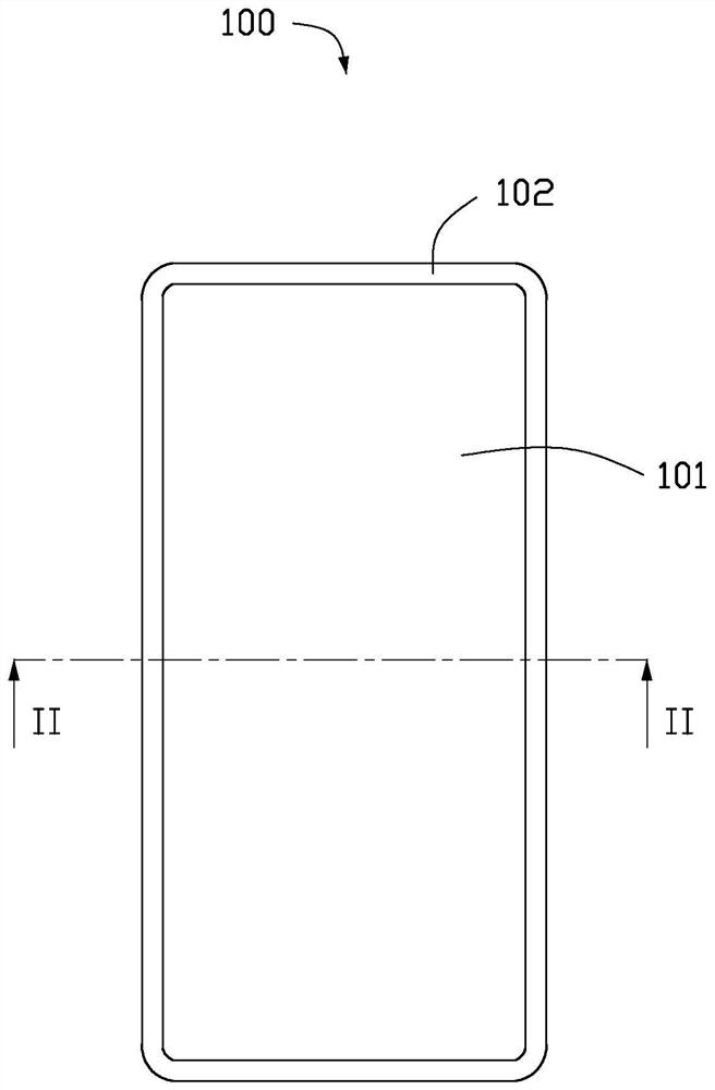
[0024]Such asfigure 1 As shown, the display device 100 provided by the embodiment of the present invention defines a display area 101 and a non-display area 102, and the non-display area 102 surrounds the display area 101.
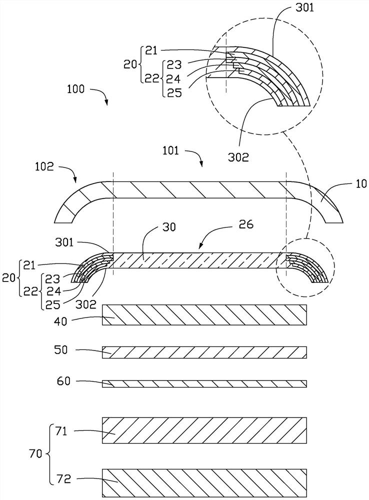
[0025]Such asfigure 2 As shown,figure 2 forfigure 1 Sectional view along the II-II tangent line. The display device 100 includes a cover plate 10, a decoration film 20, a first transparent insulating glue layer 30, a polarizer 40, a touch module 50, a second transparent insulating glue layer 60 and a display module 70. Wherein, the decorative film 20 is disposed corresponding to the non-display area 102 and surrounds the display area 101.
[0026]The first transparent insulating glue layer 30 is formed in the opening 26 and extends from the opening 26 to the non-display area 102 to wrap the opposite surfaces of the decoration film 20. The first transparent insulating glue layer 30 has a first side 301 and a first side 301 and 302 on both sides. The cover plate 10 is d...
PUM
 Abstract
Description
Claims
Application Information