Horizontal diode device

A technology of lateral diodes and devices, applied in semiconductor devices, semiconductor/solid-state device manufacturing, electrical components, etc., can solve the problems of low forward current density and poor reverse blocking ability.

Active Publication Date: 2018-12-21
UNIV OF ELECTRONICS SCI & TECH OF CHINA
View PDF6 Cites 0 Cited by
  • Summary
  • Abstract
  • Description
  • Claims
  • Application Information

AI Technical Summary

Problems solved by technology

[0006] Aiming at the problems of low forward conduction current density and poor reverse blocking ability of the above-mentioned traditional lateral silicon carbide super-barrier diodes, the present invention proposes a lateral Diode device and method of making the same

Method used


Image

  • Horizontal diode device
  • Horizontal diode device
  • Horizontal diode device

Examples


Embodiment 1

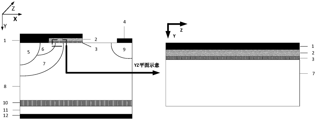
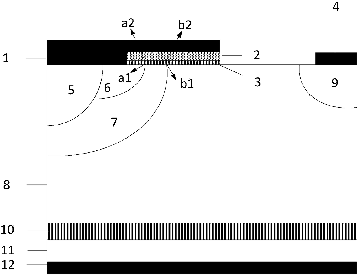
[0067] This embodiment takes the structure of a 600V lateral diode device as an example, as figure 2 As shown, the cellular structure of the lateral diode device in this embodiment includes a substrate electrode 12, an N-type silicon carbide substrate 11, a dielectric layer 10, and an N-silicon carbide drift region 8 arranged sequentially from bottom to top, and N- A P-type silicon carbide base region 7 is set on one side of the top layer of the silicon carbide drift region 8, and an N+ silicon carbide drain region 9 is set on the other side; the upper surface of the N+ silicon carbide drain region 9 has a cathode metal 4; the top layer of the P-type silicon carbide base region 7 is arranged side by side Set P+ silicon carbide contact region 5 and N+ silicon carbide source region 6, N+ silicon carbide source region 6 is located on the side close to N+ silicon carbide drain region 9 and its depth does not exceed the depth of P+ silicon carbide contact region 5; N+ silicon carbi...

Embodiment 2

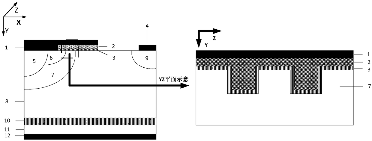
[0070] This embodiment makes a certain degree of modification to embodiment 1, and its structure is roughly the same as that of embodiment 1, the difference is that there is also an anode metal 1 inside the groove structure, that is, the depth of the lower surface of the anode metal 1 is deeper than that of the groove at the top of the structure, such as Figure 7 shown. This improvement can reduce the gate resistance, increase the charging speed of the gate charge, and further optimize the rectification performance of the device, so that the gate control capability of the device is further improved.

Embodiment 3

[0072] This embodiment makes some modifications to Embodiment 1 and Embodiment 2, and its structure is roughly the same as that of Embodiment 2. The difference is that in this embodiment, the gate structure extends toward the N+ silicon carbide drain region 9, And one end of the polysilicon 2 close to the N+ silicon carbide drain region 9 is in contact with the upper surface of the N- silicon carbide drift region 8 to form a Si / SiC heterojunction with rectification characteristics, and the junction width is about 0.1 μm to 0.3 μm, such as Figure 8 shown. The lateral diode device in this embodiment has a three-dimensional super-barrier structure and a Si / SiC heterojunction, and the heterojunction significantly increases the forward conduction current level of the diode in this embodiment.


PUM


Abstract

A lateral diode device belongs to the technical field of power semiconductor device. The cell structure comprises a substrate electrode, an N-type semiconductor substrate, a dielectric layer and an N-Semiconductor Drift Region which are successively arranged from bottom to top, A P-type semiconductor base region is arranged on one side of the top layer of the N-semiconductor drift region, and an N+ semiconductor drain region is arranged on the other side; An upper surface of the N + semiconductor drain region is provided with a cathode metal; A P + semiconductor contact region and an N + semiconductor source region are arranged side by side on the top layer of the P-type semiconductor base region, and the N + semiconductor source region is located on a side close to the N + semiconductordrain region; The N + semiconductor source region, P-type semiconductor base region and The upper surface of the N-semiconductor drift region is provided with a trench structure, and the trench structure has a gate structure including a dielectric layer, polysilicon and an anode metal which are arranged from bottom to top. An upper surfaces of the P + semiconductor contact region and the N + semiconductor source region have an anode metal. The invention has the characteristics of high forward current density, low on-state loss, high rectification efficiency and high voltage blocking ability.

Description

technical field [0001] The invention belongs to the technical field of power semiconductor devices, and in particular relates to a lateral diode device structure. Background technique [0002] The history of mankind is a history of facing challenges from nature. With the continuous expansion of the depth and breadth of the human industrial revolution, people are constantly facing various crises while enjoying the convenience brought by the fruits of industrialization. As the "blood" of industry, the sustainable utilization of energy resources has always been valued by countries all over the world. The increasing consumption of energy resources has also made people feel the "energy crisis". While seeking new energy as an alternative to fossil energy, people are also thinking about how to maximize energy utilization. Electric energy is the main energy that human beings can directly use, and the power system that manages electric energy is a key way for human beings to impro...

Claims


Application Information

Patent Timeline
Patent Type & Authority Applications(China)
IPC IPC(8): H01L29/861H01L29/06H01L21/329
CPCH01L29/0688H01L29/66136H01L29/8618
Inventor 张金平邹华罗君轶赵阳刘竞秀李泽宏张波
Owner UNIV OF ELECTRONICS SCI & TECH OF CHINA
Why Eureka
Try Eureka