

Device for changing a surface shape of an optical element by means of electron irradiation
A technology of optical components and electron radiation, which is applied in the field of optical components and can solve problems such as deviation
Active Publication Date: 2018-12-21
CARL ZEISS SMT GMBH
View PDF3 Cites 2 Cited by
- Summary
- Abstract
- Description
- Claims
- Application Information
AI Technical Summary
Problems solved by technology
[0008] A problem during the treatment of the surface of an optical element by electron radiation is that the actually achieved shape correction of the surface
Method used
View moreImage
Smart ImageViewing Examples

Examples
 PUM
 Abstract
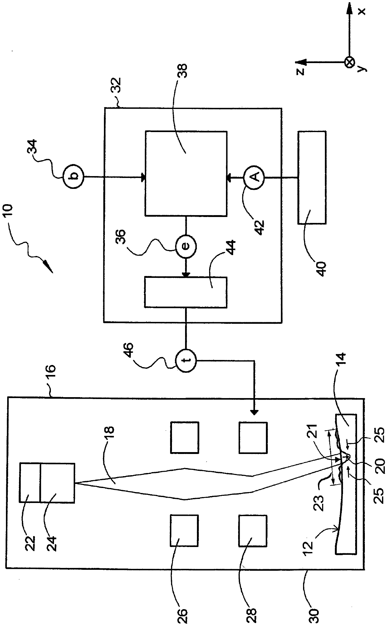
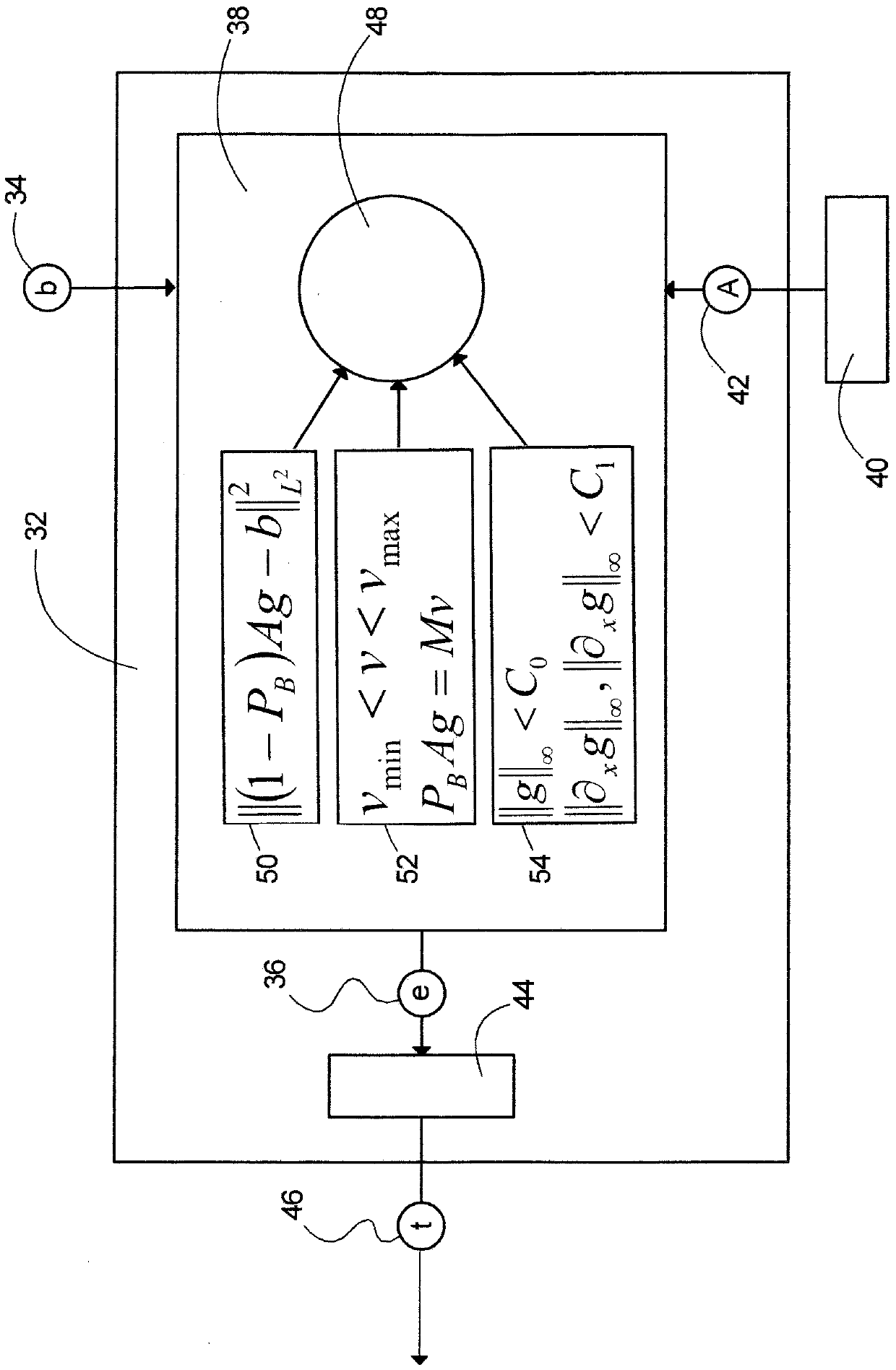
The invention relates to a device (10) for changing the shape of a surface (12) of an optical element (14) by means of electron irradiation. The device (10) comprises an electron irradiation device (16) for irradiating electrons onto the surface (12) with a spatially resolved energy dose distribution (36) in order to produce local material compressions in the optical element (14). The device (10)further comprises a controller (32) for ascertaining a spatially resolved energy dose distribution (36) from a specified target change (34) in the surface shape of the optical element (14) by means ofan optimization process with a minimization of a quality function (50) such that a difference between the target change and an actual change in the surface shape of the optical element produced on the basis of the ascertained specification is minimized. The quality function (50) contains a conversion term (42) for converting a local compaction, which describes a material compression in the regionof the surface (12), into a resulting shape change of the surface (12). The conversion term (42) takes into consideration both a surface depression (20) produced by the local compaction as well as adeformation of the surface (12) produced on the basis of forces acting parallel to the surface (12). The invention further relates to a corresponding method and a projection objective for microlithography.
Description
[0001] Cross References to Related Applications [0002] This application claims priority from German patent application 10 2016 203 591.6 of March 4, 2016. The entire disclosure of this patent application is incorporated into this application by reference. technical field [0003] The invention relates to a device and a method for modifying the surface shape of an optical element by electron radiation. Furthermore, the invention relates to a projection lens for microlithography and an inspection unit for inspecting a substrate for microlithography, such as a reticle inspection unit or a wafer inspection unit, each comprising an optical element manufactured by the above-mentioned method. Background technique [0004] It is known from the prior art that material densification occurs in the case of amorphous materials due to electron radiation. One approach in this regard consists in the compression of the material that occurs due to the redistribution of electron bonds near...
Claims
Login to View More Application Information
Patent Timeline
 IPC IPC(8): G02B1/12G02B5/08G03F7/20
CPCG02B1/12G02B5/0891G03F7/70958G03F7/70266G03F7/70308G03F7/70316G03F7/70033G03F7/70616
InventorW.保尔斯F.阿勒斯M.韦泽
OwnerCARL ZEISS SMT GMBH